Introduction
With the increase in power density resulting from advancements insemiconductor packaging technologies comes the issue of heat dissipation. Heatis generated as a result of electrical energy being converted to thermal energyduring circuit activities. The junction temperature of a chip directly affectsthe performance of the circuits and the reliability of packages.

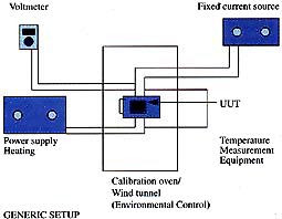
Figure 1: Diagram of electrical test method(ETM)
It is very important therefore that the junction temperature of each packagebe known as accurately as possible through direct measurement. It is furtherimportant that such measurement be repeatable, and comparable to measurementsmade on other packages since it constitutes a measure of performance. Andlastly, it is important that the technique of measurement be universally appliedin the industry in order to achieve meaningful and unbiased comparison ofsimilar packages. To this end, the Joint Electron Device Engineering Council (JEDEC), under the Electronic Industries Association (EIA), is creating athermal measurement standard for IC packages. The Council has recently publishedthe first phase of this standard that is expected to achieve the above goalsupon completion.
The purpose of this article is to briefly summarize the essence of thisstandard, and evaluate some of the issues that are yet to be addressed.
JEDEC Standard
The JEDEC standard is being developed to create a uniform method ofcharacterizing IC packages in order to establish a frame work by which theperformances of different packages housing similar devices, or different devicesin similar packages, can be compared.
The choice of measurement technique is the electrical measurement method(ETM). ETMs are not new. They involve the use of forward voltage in temperaturesensitive devices such as diodes to determine the temperature of the junction.Many companies have been using this method in one form or another, with customsetups or standard available equipment, depending on the sophistication of theuser and the complexity of the device. Data from tests using this technique havebeen well published. Some of them are referenced at the end of this article [1,2 & 3]. What the JEDEC standard does differently, however, is to clearlyrecommend specific environmental conditions, measurement techniques, fixturing,heating power guidelines, and specific wiring and connection configurations forboth thermal dice and active devices.
A unique aspect of the standard is that it calls out for specific test boarddesign. This design specifies the geometry and contacts of the board based onthe number of pins, pin sizes and package body sizes. This is aimed atstandardizing the impact of printed circuit boards on the thermal performance ofthe package itself.
The standard consists of different documents some of which are still beingdeveloped. The approved documents to date include JESD51(Overview), JESD51-1(TheElectrical Test Method), JESD51-2 (Natural Convection Environment Standard) andJESD51-3 (Low Thermal Conductivity Test Board for Leaded Surface MountPackages). So far, only surface mount boards have been addressed. The JEDECJC-15.1 subcommittee which is responsible for developing this standard, ispresently working on board specification for through-holes and other packages.
Other documents that are yet to be completed and approved include InfraredTest Method, ETM Implementation, Forced Convection, Heat Sink, High ConductionThermal Test Boards, Resistive Heating Thermal Test Die, Active Device ThermalTest Die, and Thermal Modeling. The list may grow in the future to accommodateinputs from the industry and changes in packaging technologies.
Industry Review
Since the approval of the first phase of the standard, reviews have beenvery positive. Most of the major semiconductor companies have either started touse it or are gearing up to comply. There have also been some issues raised bysome potential users of the standards. The JEDEC-JC15 Committee plans to addressmost of them in subsequent developments of the standards, but we can look at afew of them now.
Issues Raised on Standard
The issues discussed herein are from the author’s personal experience indesigning to the standard and from questions raised by colleagues in theindustry:
1. Relevance to non-JEDEC packages
Should non-JEDEC package designers worry about this standard? Since thepurpose of the standard is primarily to create a framework against which “differentpackages carrying similar devices, or similar packages carrying differentdevices” can be compared and evaluated, it is essentially notpackage-specific. Thus, the author suggests that in order to give anindustry-wide validation to their test data, non-JEDEC packages should also betested to the same standard.
2. Non traditional packages
Does the standard address complex, advanced packages? The JEDEC committeeintends to cover as many packages as possible in future revisions of thestandard. However, for packages that are highly customized and specialized, thetest method, wiring configurations, environmental conditions and poweringguidelines, can still be applied to comply with the standard. In such cases, thepublication of the results must comply with the requirements for data correctionand presentation in the standard.
3. Ball Grid Array (BGA) test board design
Overwhelmingly most of the questions have been on this topic. In theirpublication: “Thermal Resistance Characterization of the 225 BGA” 4,John Pursel and Tom Tarter discuss some of these issues. The standard is veryclear on single layer test boards.
However, the committee has not yet addressed the issue of multiple layerprinted circuit boards (PCB’s). The design of these boards pose specialchallenges, especially BGA test boards. Depending on the number of balls and theball pitch, the PCB can quickly get very complicated. BGAs are a special casebecause the PCB is very critical to the cooling of the package, particularly inplastic BGAs because the board is the principal means of removing heat fromthese packages.
The issue is how to standardize BGA test boards. An important use of thermaldata is to enable System Designers to predict the thermal performance of theirsystems. Since the chip vendor cannot predict the board designs of all possibleusers, the vendor will like to evaluate the package itself, as independent fromthe influence of the board as possible. To achieve this, some companies use theabsolute minimum number of layers that the design will allow. This is thevendors’s perspective for worst case. However, from the users’ perspective, thesetup should reflect actual operating conditions, especially if this issignificantly different from the vendor’s test conditions. Lastly, there iscost. Trying to reduce the layers to a minimum often involves having to useminimum trace widths and air gaps. In the PCB industry, any trace width lessthan 6 mils could exponentially increase the cost of fabrication; therefore,even from the vendor’s perspective, the choice of design must also reflect thecost of fabrication. The question then is: which perspective should be used inobtaining test results for publication and comparing with similar device/packageperformances? The JEDEC Committee might consider the minimum layer approachusing standard trace widths and air gaps, and no thermal enhancements such asthermal vias, for the Vendors’ Perspective Test (VPT). For a System Designer whowants to evaluate his package for operational conditions, this may beunrealistic. To design for a User Perspective Test (UPT) the board must reflectthe user’s operating specification.
JEDEC is still working on finalizing this aspect of the standard. Inanticipation of some of these issues the standard calls out for a “completestatement of test conditions and environmental conditions” for presentationof thermal data to be complete and meaningful. What JEDEC may consider as mostcritical could be that the instrumentation be set up properly, the Device UnderTest (DUT) be designed to spec, the test be performed exactly as specified, andall non-specified parameters be clearly documented and published with the resultsuch that the test can be repeated by another person.
Test Methodology
The JEDEC JC-15. ETM (Electrical Test Method) application can be dynamic orstatic. Dynamic Mode involves switching from electrical parameter measurementcondition to a heating condition during which power is applied to the DUT for aspecific period of time, and then switching back to the temperature-sensitiveelectrical parameter measurement. Static mode involves heating the package tosteady state and then making temperature measurements.
The temperature sensitive electrical parameter usually takes the form of avoltage drop across a forward biased diode designed into the DUT which could bea thermal die or an active device. The measurement current for this diode isselected carefully, so that it is large enough to be reliably measured, but lowenough not to create significant package heating. This current often ranges from100µA to 5mA. Thermal dice may contain multiple diodes, strategicallylocated to monitor the temperature of different parts of the die. These chipsare also specifically designed to provide uniform heating for the purpose ofmeasuring the thermal resistance of the package. When measuring thermalresistance, total heating over the die surface should be in compliance withstandards of the Semiconductor Equipment Manufacturers International(SEMI)#G46-88 and EIA-JEDEC standards.
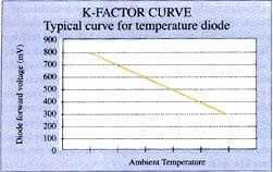
Thermal measurement involves initial calibration of the thermal dice in asteady, uniform temperature environment such as a liquid bath or a tightlycontrolled small oven. Calibration is done by measuring the electricalparameters of the measurement diode, such as the forward voltage, at a knowntemperature. Measurements of voltages at different temperatures are then made(at least two points) to obtain a proportionality constant, K(T/
V, the chip calibrationfactor.) as shown in fig 2.
Figure 2 K-factor curve
The device is then placed in still air within a specific size box (definedin the standard,) or environment of known air velocity and temperature (yet tobe defined in the standard). Junction temperature in this known environment isdetermined by measuring the diode forward voltage and using Equation (1) todetermine the junction temperature first with no power to the device, and thenwith the device powered up.
K = TJ
TSp
(1)
WhereTJ =change in junction temperature
TSp = changein electrical parameter K =
TJ
TSpConstant
The sequence of powering and taking measurement partially depends on thetype of test being performed (static or dynamic). Thermal resistance (orimpedance, for dynamic test) is the ratio of the difference between the junctionand a reference temperature, to the power added as shown in Equation (2).
| ——————————– | (2) | |
| PH | ||
| Where |
||
| PH = powerdissipation that produced change in junction temperature | ||
The reference temperature could be ambient forj-a, casetemperature for
j-cor board temperature for
j-b.If significant heating of the ambient air occurs as a result of powering up thedevice, the temperature change should be factored into the equation as outlinedin the JEDEC standard. Reference 1 contains more discussions on the ETM.
Equipment that can automatically perform this test is available in themarket. There are also companies that design and supply the JEDEC Thermal TestBoards and perform the tests.
Conclusion
This standard is a very welcome step towards creating uniformity in thecharacterization of packages. The review of the standard so far confirms thisfact. Package thermal performance is becoming increasingly significant as chipsbecome faster and packages get denser. All the more reason to establish auniversal method of measuring this important aspect of electronic packaging.
The approved documents and information on the others, questions about thestandard, details of data collection, integrity and accuracy can be obtained bycontacting the Electronic Industries Association (EIA), 2500 Wilson Blvd.,Arlington, Virginia 22201, USA. The JEDEC JC15 Committee also encourages inputsin the form of comments, suggestions, or desire to participate in the shaping ofthe standard.
References
1. Bernie Seigal. Elements of Device ThermalCharacterization, Electronic Cooling, vol 1, number 1, June, 1995.
2. H. Shaukatullay and Michael A. Gaynes, Experimental Determination ofthe Effect of Printed Circuit Card Conductivity on the Thermal Performance ofSurface Mount Electronic Packages, IEEE SemiTherm Proceedings, 1994.
3. Darvin Edwards, Ming Hang, Bill Sterns, Thermal Enhancement of ICPackages, IEEE SemiTherm Proceedings, 1994.
4. John W. Pursel, Tom Tarter, Thermal Resistance Characterization of the225 BGA. Advanced Micro Devices.


