Figure 1. Various leadframe and BGA packages
Introduction
The well-established trend within the electronics industry to provide everincreasing computing power at less cost seems to defy the laws of economics.However, this industry has not been able to suspend the laws of physics. Eachcalculation by each of the millions of transistors in the modern personalcomputer is accompanied by the generation of heat. The reduction in theoperating voltage of circuits has not been able to reverse the trend towardshigher power per chip caused by increased chip complexity and operatingfrequency.
As electronics has become all-pervasive, the need for reliability hasincreased. The operating temperature of integrated circuits must be kept withinstrict limits to prevent the premature demise of these circuits as a result ofthermally-activated failure mechanisms.
In the face of this incredible evolution, the primary function ofmicroelectronic packaging has not changed to provide an electricalinterconnection between the microscopic circuitry of the integrated circuitdevice to the much larger traces on the systems printed circuit board (PCB).Due to the increased power generated by today’s microcircuits, a necessarysecondary role of the package is to conduct heat to other parts of the system,whence it can be transmitted to the ambient air.
It is a tribute to the ingenuity of modern packaging technology that, to alarge extent, changes in package design alone have been able to provide therequired improvements in system thermal performance. These design improvementswere largely an unintended consequence of the adoption of surface-mounttechnology and the subsequent use of multi-layer system PCBs.
These PCBs, that incorporate ground and power planes in their construction,provide much more heat spreading than the older through-hole PCBs, which lackedthese planes. However, in many applications, particularly in portableelectronics and those involving high performance microprocessors, system-levelthermal solutions are becoming more necessary. It is a near certainty that thistrend will grow in significance.
Overview of package designs
This article will focus on package designs of significance for consumerapplications. As such, the discussion will be limited to plastic packaging.These packages will be divided here into two major classes: 1) those based onleadframe technology and 2) those based on laminate technology.
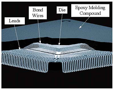
In leadframe packages, the conductors consist of leads that have beenproduced from a single copper alloy strip by stamping or etching. Theseconductors are thick enough to impart mechanical rigidity to the packagecomponents during assembly. The typical leadframe package has leads thatcontact the PCB at its periphery either along two opposite sides (dual-sidedpackages) or on all four sides (quad packages). Various leadframe package areshown in Figure 1. The internal design of a quad package is illustrated inFigure 2.
Figure 2. Perspective view of Quad Flat Package, withepoxy molding compound partially cut away to show internal construction ofpackage
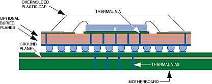
By contrast, laminate packages contain a PCB, produced by a refined versionof the same technology used to produce system PCBs. The conductors consist oftraces etched in copper foil bonded to a reinforced polymer substrate. PCBtechnology permits laminate packages to have several layers of conductors andplanes with the inter-layer connection provided by through-hole plated vias.Laminate packages normally have an area array of leads. The most commerciallysignificant laminate package in today’s technology is the Ball Grid Array (BGA)package. In this case, the leads consist of balls of solder. Figure 1 depictsa number of BGA package formats. Figure 3 illustrates the internal design of aplastic BGA package.
Figure 3. Diagram of a PBGA package, soldered to aPCB
In both leadframe and BGA packages the die, the bond wires, and thecentrally-located portion of the conductors are encapsulated in plastic moldingcompound.
Heat transfer fundamentals
There are a large number of different configurations of packages possible inthe varied applications of today. In order to present data that will bestclarify the role of the package in thermal management, the present discussionwill assume an industry-standard test environment. In this environment, asingle package is mounted to the center of a test PCB, whose dimensions andmetal content are maintained to within precisely defined tolerances, to preventexcessive variability in the test results due to variations in test PCBconstruction. The primary factors important in system applications arerepresented in the simplified standard test environment, namely, conductionwithin the package from the die to the external surfaces of the package,conduction in the board, and heat exchange to the ambient by means of convectionand radiation from the top of the package and the top and bottom of the board.Figure 4 illustrates these primary heat flow paths for a leadframe packagemounted to a test PCB.
Figure 4. Primary heat flow paths for a leadframepackage mounted to a PCB
It is a characteristic of surface-mount packages tested in the standardenvironment that upwards of 70% of the generated heat flows to the air throughthe board. The presence of metal planes in the test PCB can increase the valueto over 90%. Since the primary path to air in the standard test environment andin most applications is through the board, the principal method of increasingthe thermal performance of a surface mount package is to decrease the thermalresistance for heat to flow from the die to the leads. The subsequent sectionswill explore the impact of design variations on the thermal performance of bothleadframe and laminate packages.
In the single-package test environment, it is customary to rate the thermalperformance of a package by means of a thermal resistance value, called
JA(pronounced Theta JA). It represents the thermal resistance for the flow ofheat between the junction (the electrically active surface of the chip) to theair by all possible paths.
JA includesthe contribution of the package, the PCB, and the heat exchange to the air. Itis defined as:
JA = (TJ– TA)/P
(1)
where TJ is the junction temperature, TA is theambient air temperature, P is the total power dissipated by the chip. In SIunits,
JAhas units of °C/W.
JA canbe viewed as a figure of merit representing the thermal performance of apackage, with the lower number representing better thermal performance. Hence,its primary value is that it provides a means of ranking packages in order oftheir thermal performance. The reader is cautioned against using Equation (1)in estimating the thermal performance of a package in an actual application.
Thermal performance of leadframe packages
The relationship between the design of a leadframe package and its thermalperformance is illustrated by using high-leadcount quad flat packages (QFPs) asexamples. In each example, the cooling mode was that of natural convection.Except as noted, the test board used in the analysis is a 4-layer PCB. Thethermal performance of this package family can be used as a baseline forcomparing that of the BGA packages.
Standard leadframe packages
In a typical leadframe package the die is attached using adhesive to a pad,which is separated from the inner tips of the leads by a small gap. Heat flowfrom the pad to the leads occurs by means of the encapsulating plastic moldingcompound, normally a material with a low thermal conductivity.
Most leadframes are fabricated from copper alloys of relatively high thermalconductivity. Hence heat flow within the pad and along the leads is ratherefficient. The limiting factor in the thermal performance of leaded packages isthe thermal resistance of the molding compound between the pad and the leads.The remainder of this section explores the effect of three important designparameters for standard leadframe packages.
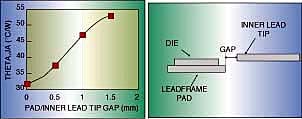
Pad/inner lead tip gap
The expectation that
JAwould be a sensitive function of the gap is consistent with the understanding ofthe plastic molding compound as the limiting factor in heat flow from the die toboard. This is borne out by Figure 5, which indicates an increase in
JA of about14 °C/W for every mm of increase in the gap between the pad and the innerlead tips. Normally, this gap is between 0.7 and 1.0 mm. A smaller gap is notpractical due to limitations in fabricating the leadframe, among otherconsiderations.
Figure 5. Relationship between the thermalperformance of a 28 mm, 160 lead QFP and the pad/inner-lead tip gap. Computersimulation. Single-layer test PCB. [1]
Leadframe thermal conductivity
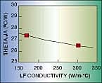
Consistent also with this picture is the expectation that once the thermalconductivity of the leadframe is large enough to cause the molding compound tobe the limiting thermal factor, additional increases in the thermal conductivityof the leadframe bring diminishing returns. Figure 6 confirms this expectation.A near doubling of the thermal conductivity of the copper leadframe from 170 to301 W/m-°C reduces
JAby only about 1 °C/W.
Figure 6. Relationship between the thermalperformance of a 176 lead, 24 mm TQFP and the leadframe thermal conductivity.Test result. [2]
Pad Size
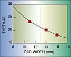
The pad size is dictated primarily by the die size and the requirement thatthe bond wire length not exceed certain limits. Hence, it cannot be changed dueto thermal considerations. However, in those cases in which an increase in diesize justifies an increase in the pad size, an improvement in the thermalperformance of the package will result. For the thin QFP (TQFP) represented byFigure 7,
JAdecreases by approximately 1 °C/W for each mm of increase in the pad size.This reduction in
JAresults from the longer perimeter of molding compound around the pad as its sizeis increased. This translates into larger cross-sectional area for heat flowacross the molding compound to the inner lead tips and hence, a lower thermalresistance.
Figure 7. Relationship between the thermalperformance of a 208 lead, 28 mm TQFP and the pad width. Test result. [3]
Thermally-enhanced leadframe packages
In the preceding examples, the variations in design having the largestinfluence on the package thermal performance are those which most affected thethermal resistance between the pad and the leads, namely the gap and the padsize. However, as discussed, the choice of these parameters is determinedprimarily by factors other than thermal considerations. The lesson to belearned is that a high-thermal-performance leadframe package should have a smallthermal resistance between the leads and the pad.
One method of achieving this end while maintaining the pad/leadframe gap andpad size within practical limits is by the insertion of a metal plate into thepackage. The metal plate contacts the pad and overlaps the leads. The thermalresistance between the leads and the metal plate is much less than that betweenthe pad and the leads in the standard package. This is due to the fact thatthere is a greater area of molding compound participating in the heat flowbetween the metal plate and the leads than there is between the pad and leads inthe standard package. There are two types of metal plates that can be insertedor “dropped” in the standard package (illustrated in Figure 8): 1) athin plate which is encased in the molding compound during assembly and 2) athicker plate whose bottom surface remains exposed after assembly. The platesin these two designs are commonly referred to as a heat spreader and a heat slug[4], respectively.
An enhanced variant of the drop-in heat slug is one in which the die isdirectly attached to the slug by means of adhesive tape [5] and the leadframe,minus the pad. This integral heat slug design is illustrated in Figure 8. Alsoin Figure 8, the thermal performance of these three enhanced packages iscompared to that of the standard QFP. The reduction in
JA affordedby these various enhancements varies between 53 and 62%. The 62% reduction in
JAtranslates into more than a doubling of the power which can be dissipated by thedie in the enhanced package compared to that for the standard package.
It should be noted that it is possible to achieve a level of thermalperformance comparable to that of the drop-in heat spreader by the use of amolding compound whose thermal conductivity has been enhanced to a level aboutfour times that of the standard, silica-filled compound. It is reasonable toexpect that the use of thermally-enhanced molding compounds will increase in thefuture as reliability issues are resolved and the material costs drop.
Thermal performance of BGA packages
Figure 8. Comparison of the thermal performance of 3enhanced package designs with the standard one. 304 lead, 40 mm MQFP package.A cross-sectional drawing of each package design is positioned to the right ofthe corresponding item on the graph. Test results. [6,7]
There are two thermal enhancements commonly employed in the design of anovermolded plastic BGA (PBGA) package, both illustrated in Figure 3: 1) theaddition of thermal vias and centrally-located thermal balls under the die, and2) the addition of metal planes in the package laminate. The thermalperformance of a standard PBGA package is compared to that of an otherwiseidentical package, containing one or both of these enhancements in Figure 9.Each of these designs contains 352 peripheral balls. The designs with 36thermal balls are described as 388 lead packages. Figure 10 illustrates theball configurations for these packages.
Figure 9. Thermal performance comparison, variousPBGA designs. 35 mm package. Test results. [8,9]
Figure 10. Ball matrix configurations for (a) 352lead and (b) 388 lead PBGA packages
In the two-layer laminate configuration, the presence of the thermal ballsproduces a significant reduction in
JA. Thebest thermal performance, however, is provided by the configuration with thefour-layer laminate. The addition of thermal balls to the four-layer designprovides only a minor improvement in the thermal performance. The enhanced heatspreading afforded by the 4-layer design offers effective thermal coupling toall of the solder balls in the package. Hence, in this design, its thermalperformance is only marginally affected by the addition of the thermal balls,representing less than 10% of the total number of balls.
An alternative design, the SBGA package*, which contains a copper-alloyheatspreader in a die-down design is also represented in Figure 9. The directattachment of the die to a copper-alloy heatspreader offers a level of thermalperformance greater than that afforded by the PBGA designs considered here. Itshould be noted that the range of thermal performance spanned by all of the BGApackages in Figure 9, corresponds approximately to that of the QFP packages inFigure 8.
Enhancement of the thermal performance of BGA packages is achieved using thesame principle operative in the QFP designs: the reduction of the thermalresistance between the package and the board.
Conclusions
The design of leadframe and laminate packages has a profound effect on thepackage thermal performance. By optimizing the package design to minimize thethermal resistance between the die and the system PCB, it is possible for athermally-enhanced package to have double the power handling capability of theun-enhanced package.
*SBGA or SuperBGA is a registered trademark of Amkor Electronics
Acknowledgments
The assistance of Lucian Hand in performing the thermal measurements and ofMoe Perez and Andrea Regna in generating the illustrations is gratefullyacknowledged.
References
[1] M. Tanaka and Y. Takeuchi, “Thermal Analysis ofPlastic QFP with High Thermal Dissipation,” Proceedings, 42nd ECTCSymposium, San Diego, 1992, pp. 332-339.
[2] L. Hand, Amkor Thermal Test Report TT-43(Non-restricted Distribution), December 10, 1996.
[3] L. Hand, Amkor Thermal Test Report TT-19(Non-restricted Distribution), March 18, 1996.
[4] The MQFP with the drop-in heat slug is marketed underthe trade name PowerQuad( 4 by Amkor Electronics.
[5] The MQFP with the integral heat slug is marketed underthe trade name PowerQuad(2 by Amkor Electronics.
[6] L. Hand, Amkor Thermal Test Report TT-41(Non-restricted Distribution), September 19, 1996.
[7] L. Hand, Amkor Thermal Test Report TT-29(Non-restricted Distribution), July 23, 1996.
[8] L. Hand, Amkor Thermal Test Report TT-27(Non-restricted Distribution), July 22, 1996.
[9] L. Hand, Amkor Thermal Test Report TT-32(Non-restricted Distribution), July 18, 1996.
Copies of Amkor Thermal Test Reports are available onrequest from the author. [A1]

