Continuous improvements in the cooling of electronic systems will berequired to keep pace with the rapid development of higher power chips.Currently, effective cooling relies (in part) on high surface area heatexchangers. Further improvements could be realized by increasing thesurface area of these devices. However, increasing the size of heatexchanger components is not a viable option, since system space isextremely limited. Therefore, creative methods must be developed toincrease effective surface area, without increasing the size of the parts.Microscopic texturing is one such method.
Microscopically textured surfaces not only increase surface area, theycan also substantially improve emissivity (radiative cooling), if surfacefeatures are of the correct size and shape. Although conventionalmicroscopic texturing processes (e.g. chemical etching) can be used toincrease surface area, they do not provide sufficient control over surfacefeature morphology to permit formation of optimal surface structures.
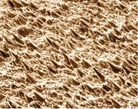
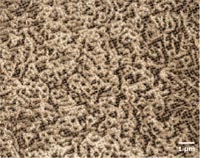
Ion beam bombardment is used to selectively etch materials inapplications ranging from electronic substrate patterning to the creationof high-surface-area pacemaker electrode tips. It is based on a phenomenonknown as sputtering, which is the process of removing material from asurface at the atomic level due to collisions between energetic (keV) ionsand substrate atoms. Since it is done on so fine a scale, the processprovides a great degree of control over surface features. In principle, itcan be used to create almost any type of surface topography that isdesired, whether smoother or rougher than the original surface. Examplesof ion beam textured surface are shown in Figure 1.
 |
 |
| Figure 1. Examples of ion beam textured surfaces. A wide range of different surface features can be produced using the ion beam texturing process. | |
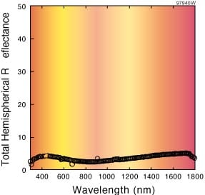
A successful application of ion beam texturing has been the creation of highly textured, light absorbing surfaces for telescope baffles. In thisapplication, a number of different materials, such as titanium andaluminum, have been textured to the degree that they absorb almost allincident light. According to Kirchhoff’s law, a highly light absorbingsurface is also highly emissive (at the same wavelengths that it absorbs).Figure 2 shows a total hemispherical reflectance spectrum from an ion beamtextured aluminum surface. This material absorbs over 90% of the incidentradiation. Such a surface would also be a highly effective emitter ofradiation across these wavelengths.
The reason that surfaces texture under ion bombardment is that thesputtering process is extremely sensitive to substrate materialvariations. In general, different materials sputter, or erode, atdifferent rates. Even different phases of a given material or differentcrystal orientations can exhibit different sputtering rates. Therefore,any material that is not perfectly homogeneous, either in elemental orphase composition, will form a “natural” texture that isdependent on composition and distribution of substrate atoms. This texturemay be enhanced or further controlled by “seeding” the substratewith impurities that sputter at a slower rate than the substrate material.
Figure 2. Total hemispherical reflectance for an ion beam texturedaluminum surface. This particular surface absorbs over 90% of the incidentlight across a wide range of wavelengths. The spectrum implies that thesurface is also highly emissive. A highly textured surface, such as theone that produced this spectrum, would be ideal for electronic cooling dueto significantly increased surface area (enhanced convective cooling) and increased emissivity (enhanced radiative cooling).
The size, shape, and distribution of surface features formed by ion beam texturing also depends strongly on the treatment conditions, such as thetype of ion that is used to bombard, the surface and its energy, the levelof the vacuum in the treatment system, the partial pressures of impuritygasses that are present, etc. These factors, when properly controlled, canbe used to tailor surface features to obtain a desired morphology.
For electronic cooling applications, a surface with features thatincrease emissivity in the infrared should significantly increase theefficiency of radiative cooling. Typically, surface features of a givensize most effectively absorb radiation with wavelength about the same sizeas the features. Therefore, creating a surface with features ranging fromapproximately one to ten micrometers should very effectively emit infraredradiation (heat). At the same time, the increased surface area provided bythe treatment should also enhance the efficiency of convective cooling.Such a treatment has potential for creating high efficiency, low-profileheat exchangers for use in high-end immersion cooling applications.


