Introduction
Plastic components are designed so that the heat is dissipated by forced or natural convection. The use of plastic packages under conditions where neither cooling method is available introduces new challenges.
High heat-dissipation plastic packages require a large-area solid heat sink in order to transfer the heat into the copper thermal lands on the printed circuit board (PCB). The difference in temperature between the component and the PCB must be as small as possible and this can be achieved by having a highly conductive thermal interface.
The purpose of this work is to investigate a standard thermal interface assembly method between the components and the PCBs. As an example, the thermal interface under a 208 Lead Plastic Quad Flat Pack (PQFP) was modelled using a Computational Fluid Dynamics (CFD) program.
Thermal Interface
Using a thermal interface under components is a decision which will affect the production process. If an interface is necessary, then a viable production method for a thermal interface assembly process must be developed. The assembly of components onto PCBs include component placement, wave soldering or solder-paste deposition and re-flow, cleaning, and conformal coating of the PCB. During any of these production processes the thermal interface can result in re-work which will increase the cost of the PCB. The thermal interface method, considered here, consists of thermal-paste/copper/solder interface. The copper shim is attached to the base of the component using a conductive paste. After curing the paste, the component is ready to be soldered to the PCB – not an easy process. It is beyond the scope of this article to describe the method of assembly of thermal interfaces in detail. Some of the considerations, however, can be summarized:
- There must be copper thermal lands, free of electrical vias, on the PCB onto which the solder paste can be deposited during the solder printing process.
- There must be no air traps. Otherwise during re-flow, this trapped air will cause the component to move.
- The flatness of the copper shims must be controlled, so that the component seating is accurate.
- Large tolerances between the base of the component and the tip of the leads make the thermal interface assembly process very difficult. This gap tolerance problem can be resolved by controlling the amount of solder and thermal paste.
- If the gap under the component cannot accommodate the copper shim assembly, then thermal paste will have to be used in isolation. In this case the gap under the component must be eliminated by using the correct amount of thermal paste. Gaps will cause the entrapment of contaminants such as flux, which cannot be cleaned during the production cleaning process. An air gap will also increase the thermal resistance between the interface and the PCB. This risk is eliminated when the copper shim method is used.
A photograph of the cross section of the thermal-paste/copper/solder thermal interface can be seen in Figure1.
Components That Require a Thermal Interface
Thermally sensitive components will require a thermal interface so that the heat can be transferred from the components to the copper thermal lands on the surface of the PCB. The heat is transferred from the thermal lands, through the thermal vias, to the thermal layers buried inside the PCB, which then transfer the heat to the cold walls.
Thermal Analysis of a 208 Lead Plastic quad Flat Pack (PQFP)The aim of this study was to investigate the effect of a thermal interface under a typical large plastic component.utilizing The temperature gradient and the operating temperature of a large plastic component can be reduced by utilizing a thermal interface between the component and the board instead of an air gap.
A plastic-encapsulated microcircuit consists of a silicon chip, a metal support, wires that electrically attach the chip circuits to the leads, and a plastic epoxy encapsulating material. There is a risk of package failure if the component is allowed to operate outside its limits. The potential accelerations of failures are moisture, contaminants, and temperature extremes, rates and cycles. An important factor in plastic package failures is the low thermal conductivity of plastics. The low thermal conductivity of the plastic increases the die temperature, and in a large component this can cause large temperature gradients in the package, which can result in die cracking, de-lamination, deformation of interconnections and encapsulant cracking. The choice of plastic packages must take account of their reliability, which is influenced by the differential between the package operating temperature and its temperature limits.
A Typical 208 Lead PQFP Assembly
This section discusses the materials used in the construction of a typical 208 Lead PQFP. The package consists of the plastic encapsulant, the lead frame, the die, the bond wires and the die attach.
The Lead Frame
The lead frame consists of a die mounting paddle and lead fingers. The purpose of the die paddle is to mechanically support the die during package manufacture. The lead fingers connect the die to the external circuitry.
The lead frame is usually made from a Copper alloy such as Cu-Fe, Cu-Zr or Cu-Mg. The thermal conductivity of these alloys can be seen in Table 1.
| Alloy Group | Thermal Conductivity at 20 C (W/mK) |
| Cu-Zr | 380 |
| Cu-Fe | 200-260 |
| Cu-Mg | 344 |
Table 1: Properties of common lead frame materialsDie Attach Materials
Die attach bonding is used to mechanically attach the die to the lead frame, and also to provide a heat flow path to the lead frame. A typical adhesive is a thermally conductive epoxy composite with a thermal conductivity of 0.8 W/mK. The epoxy adhesive layer is typically 25µm thick.
The Bond Wires
Wire bonding is the most commonly used technique in the plastic package interconnection technology. Gold wire is the most preferred material, on account of its high oxidation resistance and low work hardening characteristics. The thermal conductivity of the gold wire is 219 W/m°C.
The Plastic Encapsulant
In general, the majority of chip packages use Novolac-based epoxies. The moulding compound is modified by additives which improve its mechanical strength, adhesion to package components, chemical resistance, electrical resistance, coefficient of expansion match and thermal and moisture resistance in the operational temperature range.
The thermal conductivity of a typical Novolac-based epoxy is 0.67 W/mK with a glass transition temperature of 150°C.
The Thermal Interface
The thermal interface assembly is outlined in Table 2.
| Material | Thickness (mm) |
| Thermal Paste | 0.1524 |
| Copper | 0.2540 |
| Solder | 0.1016 |
Table 2: Thermal interface assembly
CFD Model
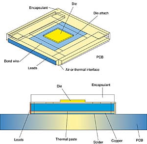
The wire bonds and the leads were modeled as blocks. In order to achieve the correct thermal resistance, the thermal conductivities of the wire bond and lead blocks were modified in the same ratio as the cross-sectional areas of the model and the real wires. The model can be seen in Figure 2. The thermal conductivities used in the model can be seen in Table 3.
Figure2: Three-dimensional CFD model.
| Part | Model Thermal Conductivities(W/mK) |
Real Thermal Conductivities(W/mK) |
| Wire bond (gold) | 11.7 | 319 |
| Lead frame (Cu-Fe) | 116.3 | 250 |
| Air | 0.03 | – |
| Thermal-paste | 0.48 | – |
| Copper shim | 391 | – |
| Solder | 35 | – |
Table 3: Thermal conductivities used in CFDTwo different thermal interfaces were considered: thermal paste only and thermal-paste/copper/solder interfaces. The maximum power dissipation for a typical 208 lead PQFP is assumed to be 1W. Four different CFD models were constructed, and these can be summarized in Table 4.
| Model | Component | Power | Thermal Interface |
| 1 | 208 Lead PQFP | 1 | Air |
| 2 | 208 Lead PQFP | 1 | Thermal-paste/Copper/Solder |
| 3 | 208 Lead PQFP | 1 | Thermal-paste |
| 4 | 208 Lead PQFP | 1 | Thermal-paste/Air |
Table 4: CFD modelsThe components are predominantly conduction cooled. It was, therefore, assumed that the heat was transferred from the chip, through the leads and the bottom of the component, to the board by conduction only. The PCB – with typical dimensions of 0.2 x 0.15 x 0.003 m – was modeled as a block with a thermal conductivity of 15 W/mK. The boundary condition was specified at the edges of the board. The boundary temperature was chosen as +85°C with a thermal resistance of 0.4°C/W which is the value for a typical wedge lock.
CFD Results and Discussion
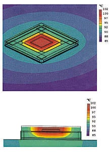
Temperature distribution for the components, dissipating 1W, with the thermal-paste/copper/solder interface, can be seen in Figure 3.
Power = 1W
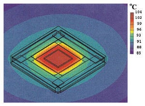
Figure 3: Thermal-paste/copper/solder thermal interface CFD modelIf the gap under the component is such that using a shim interface is impractical, then only thermal paste should be used. The temperature distribution in the PQFP if only thermal paste is used, can be seen in Figure 4.
Power = 1 W
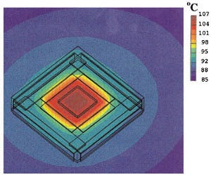
Figure 4: Thermal-paste thermal interface CFD modelThe paste must be cured before re-flow, otherwise out-gassing will occur during re-flow. It is, however, very difficult to achieve a perfect interface without any air gaps under the component when the thermal paste is cured before re-flow. In practice air gaps under the thermal paste will exist. If air gaps exist under the component, then there is a risk of trapping contaminants and flux, which cannot be cleaned during the PCB cleaning process. This air gap will also increase the thermal resistance. The air gap – 0.08 mm thick – under the thermal interface was modelled and the temperature distribution can be seen in Figure 5.
Power = 1 W
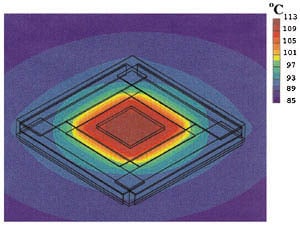
Figure 5: Thermal-paste thermal interface with an 0.08 mm air gap CFD modelThe temperature distribution in the PQFP when no thermal interface was used can be seen in Figure 6.
Power = 1 W
Figure 6: No thermal interface CFD modelThe summary of all the results can be seen in Table 5.
| Model | Power | Thermal Interface | Junction Temperature (°C) |
| 1 | 1 | Air | 113 |
| 2 | 1 | Thermal-paste/Copper/Solder | 102 |
| 3 | 1 | Thermal paste | 104 |
| 4 | 1 | Thermal-paste/Air | 107 |
Table 5: Summary of the CFD resultsThe reliability of the package is influenced by the differential between the operating temperature of the component and its maximum allowable temperature limit. The conclusion from this analysis based on the CFD results, summarized in Table 5, would be to use the thermal-paste/copper/solder interface as the temperature reduction is large. The other advantage of this type of interface is that the risk of entrapment of contaminants under the component is eliminated.
The printed circuit boards, however, must be designed with manufacture in mind. If an economically viable method of thermal interface assembly is not utilized, then the use of thermal interfaces can increase the cost of the board.
References:
| 1. | Richard van Gestel, “Reliability Related Research on Plastic IC-Packages: A Test Chip Approach” , 1990. |
| 2. | Pecht Michael G., Nguyen Luu T. and Hakim Edward B., “Plastic Encapsulated Microelectronics”, 1995. |

