Technological advances in the electronics industry have revolutionized the way the world communicates and conducts business. Today’s electronic products, from cellular phones to sophisticated imaging satellites, demand lightweight, low-cost materials that provide more functionality in less volume. To meet these challenges, electronic systems must dump large amounts of waste heat more effectively and balance the thermal stresses created by dissimilar materials.
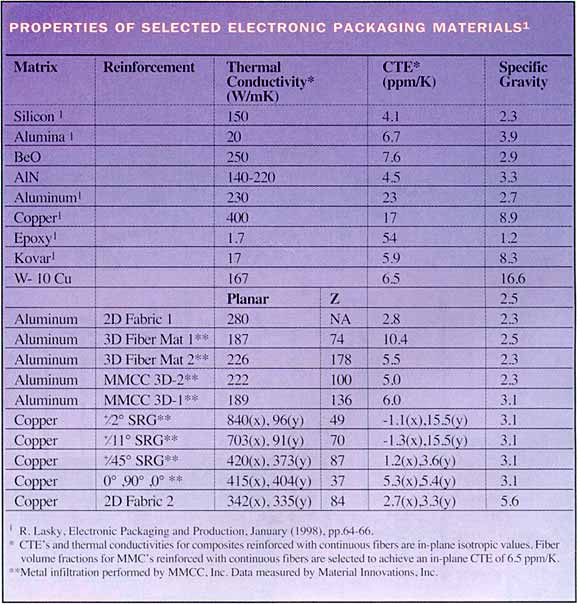
As power densities increase, reducing or eliminating thermal mismatch strains and improving the ability to dissipate heat will pose significant challenges for future electronic systems. To help meet these challenges, an alternative class of materials is being produced from graphite-aluminum and graphite-copper composites. These materials cover a wide spectrum of substrate and heat sink packaging application requirements to match the thermal expansion coefficients of Si, GaAs, and alumina.
Graphite fibers can have a thermal conductivity in excess of 1000 W/m-K with a CTE in the range of -1 to -2 ppm°C. Woven fabrics of such filters can be infiltrated with aluminum or copper to produce components with designer properties. For example, customized thermal planes of high modulus graphite fiber infiltrated with aluminum can reduce the surface CTE of organic printed circuit boards (PCBs) from 17 ppm/°C to 6 ppm/°C and provide a planar thermal conductivity of 270 W/m-K. Thus, an active thermal core for heat dissipation and low thermal mismatch stress is provided for mounted semiconductor devices, eliminating the need for internal copper planes.
In many applications, it is necessary to remove the heat in the z (through panel) direction rather than simply spreading it to the periphery. Three-dimensional woven preforms can be designed to engineer conductivity and CTE in all three-principle axes. By using carbon fiber aircraft brake technology, thick plates of porous graphite fiber can be pressure infiltrated with Al or Cu to be used as machining stock for electronic heat sink and substrate components.
To date, one of the more common packaging materials is comprised of admixtures of copper-tungsten alloys (Cu-W). By varying the copper content, CTE ranges from 6-8.5 ppm/°C, and thermal conductivity values peak at about 200 W/m-K. By comparison, Gr/Al substrates and heat sinks exceed the conductivity of Cu-W by 38% and provide a seven-fold decrease in mass (2.38 g/cc) as compared to Cu-W (18 g/cc). Hence, for weight critical applications, such as satellite telecommunications systems, a reduction in overall satellite mass can result in a less expensive launch vehicle and longer time “on line” since more propellant is available to maintain orbital position. Consequently, satellite designers are actively seeking replacement materials for Cu-W.
Each new product generation represents increasing risk for the chip designer. This risk can either relate to the uncertainty of being able to develop manufacturing solutions or result in a delay in technology development. Reducing this risk, pressure infiltrated graphite fiber reinforced aluminum and copper alloys offer system designers advantages in performance, reliability, and configurability. As the cost of graphite fibers declines and progress in preform and metal infiltration processes evolve, more applications will arise that demand the weight advantages of aluminum with variability in thermal expansion granting designers the flexibility of selecting low cost heat sink and substrate materials.


