The readers of “Electronics Cooling” are familiar with the reasons why the junction to ambient thermal resistance [1], ![]() JA or R
JA or R![]() JA, is an inadequate description of the thermal performance of an integrated circuit. Likewise, you realize that vendors cannot continue to state the integrated circuit will work at a specified ambient temperature (55°C, 70°C, 85°C, or 125°C) as device power levels increase. When an ambient temperature is specified without any other qualifying environmental conditions, the integrated circuit manufacturer must have a significant safety margin. What is needed is a more accurate description of the thermal performance.
JA, is an inadequate description of the thermal performance of an integrated circuit. Likewise, you realize that vendors cannot continue to state the integrated circuit will work at a specified ambient temperature (55°C, 70°C, 85°C, or 125°C) as device power levels increase. When an ambient temperature is specified without any other qualifying environmental conditions, the integrated circuit manufacturer must have a significant safety margin. What is needed is a more accurate description of the thermal performance.
The least complicated model for the component that captures a reasonable description of the thermal performance is a two resistor model. The two resistor model is defined in this paper as the junction-to-case and the junction-to-board thermal resistances. The junction-to-case thermal resistance, ![]() JC, determines the performance of the integrated circuit package at the limit where the major heat flow is to a heat sink. At the other limit, the majority of the heat flow is to the printed circuit board with thermal resistance described by the junction-to-board thermal resistance,
JC, determines the performance of the integrated circuit package at the limit where the major heat flow is to a heat sink. At the other limit, the majority of the heat flow is to the printed circuit board with thermal resistance described by the junction-to-board thermal resistance,![]() JB. The junction-to-board thermal resistance and its test method are defined.
JB. The junction-to-board thermal resistance and its test method are defined.
Two Resistor Thermal Model
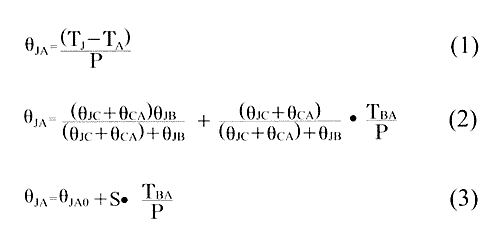
The two resistor thermal model is derived from a paper by Jim Andrews [2]. A slight simplification of this model [3] is shown in Figure 1. The integrated circuit package is modeled as a junction-to-board and a junction-to-case thermal resistance. The heat loss to the air from the package is modeled as the case-to-ambient thermal resistance. The environment of the board is represented in this model as a battery representing the board temperature rise above the ambient temperature, TBA. The board temperature rise is caused by both the power dissipation in the integrated circuit being modeled and by the power dissipation of other components on the board.
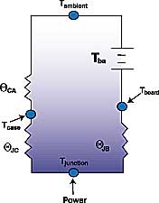
Figure 1. Two resistor model
By solving this resistor network for the junction-to-ambient thermal resistance, ![]() JA, as shown in Equations 2 and 3, one finds that
JA, as shown in Equations 2 and 3, one finds that ![]() JA can be expressed as a constant term,
JA can be expressed as a constant term, ![]() JA0, that is the junction-to-ambient thermal resistance with the board temperature held to the ambient temperature and a term that is linearly dependent on the board temperature rise above ambient divided by the package power, TBA/P. The slope of that line, S, is known as the sensitivity factor. For typical surface mount packages, the slope of that line is close to one. In other words, the junction temperature rises about 1°C for every 1°C rise in board temperature at 1 watt power dissipation. The validity of the simple model is confirmed by the ability to plot experimental measurements of
JA0, that is the junction-to-ambient thermal resistance with the board temperature held to the ambient temperature and a term that is linearly dependent on the board temperature rise above ambient divided by the package power, TBA/P. The slope of that line, S, is known as the sensitivity factor. For typical surface mount packages, the slope of that line is close to one. In other words, the junction temperature rises about 1°C for every 1°C rise in board temperature at 1 watt power dissipation. The validity of the simple model is confirmed by the ability to plot experimental measurements of ![]() JA as a function of the TBA/P.
JA as a function of the TBA/P.
To demonstrate the range of validity of the model, 272 27×27 mm PBGA and 208 28×28 mm plastic QFP packages were measured on multilayer thermal test boards with a heater pad on the bottom of the board at two power levels in the packages, two power levels in the heater pad, and at air flow between natural and 4 m/s forced convection. All data fit a straight line with about 10% scatter.
Determination of  JCand
JCand  JB
JB
The determination of the values to be used for junction-to-board and junction-to-case thermal resistance are being developed in the JEDEC JC15.1 standards committee [4]. Until an improved standard is available for ![]() JC, the recommended specifications are MIL STD 883D, Method 1012.1 [5] or SEMI G30-88 [6]. Both specifications agree that the junction-to-case thermal resistance should be measured from the junction to an “isothermal surface” obtained by placing the package on a copper cold plate (“infinite heat sink”). Unfortunately, the method of measuring the “case” temperature is inadequately defined. Both specifications assume that no correction for parasitic heat loss is required. With no heat sink, the effective thermal resistance from the top of the package to the air is usually high enough to mask minor errors in the effective junction-to-case thermal resistance. With a heat sink, a metal heat sink attached to the package provides a similar thermal environment to the measurement method.
JC, the recommended specifications are MIL STD 883D, Method 1012.1 [5] or SEMI G30-88 [6]. Both specifications agree that the junction-to-case thermal resistance should be measured from the junction to an “isothermal surface” obtained by placing the package on a copper cold plate (“infinite heat sink”). Unfortunately, the method of measuring the “case” temperature is inadequately defined. Both specifications assume that no correction for parasitic heat loss is required. With no heat sink, the effective thermal resistance from the top of the package to the air is usually high enough to mask minor errors in the effective junction-to-case thermal resistance. With a heat sink, a metal heat sink attached to the package provides a similar thermal environment to the measurement method.
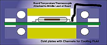
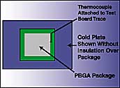
The method being considered to determine ![]() JB by the JEDEC JC15.1 committee uses a cold plate in a “ring” or “window frame” configuration clamped on both sides of the printed circuit board with the top of the package and the bottom of the board insulated as illustrated in Figures 2 and 3. The assumption is that the important thermal resistance to the board is the thermal resistance from the junction to the edge of the package where the package footprint connects to the rest of the board. Hence, the board temperature is measured by attaching a thermocouple to a trace at the edge of the package.
JB by the JEDEC JC15.1 committee uses a cold plate in a “ring” or “window frame” configuration clamped on both sides of the printed circuit board with the top of the package and the bottom of the board insulated as illustrated in Figures 2 and 3. The assumption is that the important thermal resistance to the board is the thermal resistance from the junction to the edge of the package where the package footprint connects to the rest of the board. Hence, the board temperature is measured by attaching a thermocouple to a trace at the edge of the package.
Unfortunately, the junction-to-board thermal resistance is not a thermal resistance of the package independent of the environment; it depends on the printed circuit board. The dependence on the printed circuit board design for leaded packages is relatively minor, but the effect is larger for PBGA packages with balls that are connected to metal patterns under the die. As an example, a 272 27×27 mm PBGA package (256 perimeter balls, 16 thermal balls, 2s substrate) was simulated with different board conductivities and vias in the board with the results shown in Table 1.
|
||||||||||||||||||||||||||||||||||||||||||||||||||||||||||||||||||||||||||||||||||||||||||||||||||||||||
As a result, the test method will require the use of the JEDEC specified 2s2p test board. For the typical application of this package, the printed circuit will have an effective conductivity and vias in the circuit board such that the junction-to-board resistance for this package design will be between 12 and 16°C/watt. This is a narrow enough range to make the value useful, although the engineer must be aware of the board design and make allowances.
The implications are that (1) ![]() JB is a ‘figure-of-merit’ for various packages, (2) If the standard test board is a reasonable representation of the application,
JB is a ‘figure-of-merit’ for various packages, (2) If the standard test board is a reasonable representation of the application, ![]() JB will provide an estimate of performance in the application, and (3) The board properties and how any PBGA package is connected to the board is important. Although not scientifically precise,
JB will provide an estimate of performance in the application, and (3) The board properties and how any PBGA package is connected to the board is important. Although not scientifically precise, ![]() JB will be a useful predictor of performance for the industry.
JB will be a useful predictor of performance for the industry.
Before discussing how the two resistor models would be built and used, it is important to recognize that, like ![]() JC and
JC and JT, a junction-to-board thermal characterization parameter can be defined,
JB. The junction-to-board thermal characterization parameter is determined using the board temperature measured with a thermocouple soldered to a board trace at the same location as shown in Figures 2 and 3.
Figure 2. Cross section view of the ring cold plate method to determine JB
Figure 3. Top view of ring cold plate with insulation removed.
This definition
is incorporated in the JEDEC forced convection specification. Because JB can be measured under a variety of environmental conditions and thermal test boards, it is not recommended as a replacement for
![]() JB , which will be specified more completely to reduce variability in the results for the same package from different vendors.
JB , which will be specified more completely to reduce variability in the results for the same package from different vendors.
Two Resistor Models Used in System Simulations
Given ![]() JC and
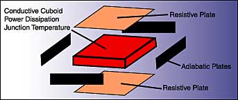
JC and ![]() JB, a package model can be constructed in a variety of thermal simulation solvers. For instance, board level solvers frequently use internal representations similar to the two resistor model [7]. Computational fluid dynamics software could use a model such as the one shown in Figure 4 [8].
JB, a package model can be constructed in a variety of thermal simulation solvers. For instance, board level solvers frequently use internal representations similar to the two resistor model [7]. Computational fluid dynamics software could use a model such as the one shown in Figure 4 [8].
Figure 4. Two resistor model using a conductive cuboid with resistive plates
top and bottom determined by ![]() JB and
JB and ![]() JC.
JC.
The package can be modeled as a highly conductive cuboid the same size as the package. The sides of the package are modeled as adiabatic. The resistance plate on the top of the model is calculated from ![]() JC; the resistance plate on the bottom of the model is calculated from
JC; the resistance plate on the bottom of the model is calculated from ![]() JB. The accuracy of this model has not been validated over a wide range of cases. Preliminary results [9] suggest an error less than 25% for calculation of the junction temperature, provided the pathological cases are avoided. I consider that useable accuracy. Cases where the model will be less accurate are the following:
JB. The accuracy of this model has not been validated over a wide range of cases. Preliminary results [9] suggest an error less than 25% for calculation of the junction temperature, provided the pathological cases are avoided. I consider that useable accuracy. Cases where the model will be less accurate are the following:
1. Most heat flow is not to the board or to the heat sink. The method of determining thermal resistances assumes heat flow to one surface or the other.
2. Significant heat dissipation occurs from the package sides (ignored for this model.)
3. For low power devices, if significant heat flow occurs from the board to the package, the internal thermal resistances for this flow are much different than the internal resistances obtained for ![]() JCand
JCand ![]() JB.
JB.
4. Adjacent heat sources are close to the package causing an asymmetric temperature field around package. Using a highly conductive cuboid for the package provides an unrealistic thermal shunt.
5. Since a cuboid the same size of the package is used for the heat source, the surface temperature and hence convective and radiation heat loss from the package are different than what would be obtained by a heat source which modeled the hot spot size on the actual package.
The compact models being developed by the DELPHI and SEED projects [10] will be more accurate and less susceptible to the problems listed above because of the greater detail contained within the model.
Conclusion
The junction-to-board thermal resistance has been defined and its usefulness in thermal simulations introduced. Any modeling or simulation technique requires compromises between accuracy and resources. The two resistor model will be less accurate but requires considerably fewer resources to implement than a 5 to 8 resistor model or a detailed model. It is anticipated that the accuracy of the two resistor model will be adequate in many situations.
Acknowledgments
In addition to the individuals cited in the references, the JEDEC JC15.1 committee (especially the round robin participants: Bruce Guenin, Chia-Pin Chiu, and Zeki Celik) and my colleagues at Motorola (Vance Adams, Dave Billings, Zane Johnson, Shailesh Mulgaonker, Koneru Ramakrishna, and Roger Stout) and Mike Eyman have contributed substantially to the concepts discussed in this paper.
References
1. JESD51-2, “Integrated Circuits Thermal Test Method Environmental Conditions – Natural Convection (Still Air),” available from JEDEC at http://www.jedec.org.
2. J. Andrews, “Package Thermal Resistance Model: Dependency on Equipment Design,” IEEE Trans CHMT, 11 (1988), pp 528-537.
3. S. Mulgaonker and H. Berg, “Thermal Sensitivity Analysis for the 119 PBGA – A Framework for Rapid Prototyping,” Proceedings of the 45th IEEE ECTC, Las Vegas, May 1995.
4. JEDEC JC15.1 is a committee of JEDEC standardization organization of EIA. Published specifications are available at http://www.jedec.org.
5. MIL STD specifications are available from Global Engineering Documents at 800-854-7179 or 303-397-7956.
6. SEMI specifications are available from Semiconductor Equipment and Materials International, 805 East Middlefield Rd, Mountain View, CA 94043 at (415) 964-5111.

