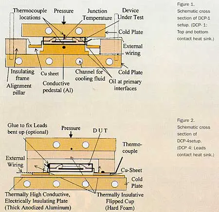
In the European project SEED (Supplier Evaluation and Exploitation of DELPHI), the methods for thermal characterization of active components developed in the predecessor DELPHI (Development of Libraries of PHysical models for an Integrated design environment) were evaluated by component suppliers. The methods were improved for practical application and extended to a large number of IC package types.
Test parts were chosen to cover a wide range of different plastic packages, including Alloy42 (FeNi42) and Cu-based lead frame material, as well as different chip sizes in the same package. Standard and thermal enhanced devices, DSO, QFP and BGA packages were studied. For all device types investigated, it was possible to generate simple resistor networks, which reproduce junction temperatures and fluxes of a detailed model for all 38 boundary conditions suggested in DELPHI with an average accuracy of 1-2%.
SEED succeeded in proposing practical methods for thermal characterization of active components, which are robust and relatively cheap (no test PCB is needed). The resulting thermal resistor network allows end users for the first time to routinely predict the junction temperatures of components in their specific applications with high accuracy.
Introduction
Power consumption of semiconductor integrated circuits increases with integration and clock frequencies. Thermal management is a critical requirement and CFD (Computational Fluid Dynamics) software has become a common tool for thermal analysis. It allows calculation of local air temperatures and heat transfer coefficients. If correct and simple thermal models of critical components are available, it becomes possible to calculate their junction temperatures with sufficient accuracy to serve as input for reliability analysis.
Unfortunately, accurate and simple thermal models do not exist. Usually, one of the two thermal resistance values JA, Junction to Ambient or
JC, Junction to Case is used to characterize the thermal behavior of the component in an application. Initially, these values were meant for comparison of IC packages in a standardized environment. Junction temperatures, heat fluxes and the so-called thermal resistances are strongly dependent on the cooling conditions. Consequently, the standardized thermal resistances are of limited value for end users, because the environment differs considerably from those in real applications.However, the component supplier cannot supply thermal data for all combinations of packages and environments. The only way to overcome this problem is to make a clear distinction between package and environment. A first step is to split
JA into two resistances. One is the package part
JB from junction to board, the other is the contribution of the board to ambient,
BA. This approach is restricted to one heat flow path via leads and PCB. Even if this is the main heat path, there is a considerable dependence on the PCB design. Despite these shortcomings,
JB could be used as a metric for comparison purposes [1].The problem of the thermal-electrical analogy is discussed in more detail in [2]. Purely unidirectional heat flow is difficult to achieve, because the heat flux from a source is in many cases dissipated in all three spatial directions involving conduction, convection and radiation as transport mechanisms. Single thermal resistance values only characterize one possible heat flow path. For a complete thermal characterization of a package more than one measurement is necessary to characterize all possible heat flow directions which a package may encounter in practice.
The DELPHI Project
The objective of the DELPHI project was to provide equipment manufacturers with simple, validated thermal models, which can be used with confidence in a wide range of environments [3,4,5].
An early statement was that a meaningful thermal simulation requires a strict separation between the responsibilities. System level packaging engineers are responsible for the component environment. Component manufacturers should supply a thermal model of a package for all practical environments. This condition is met by an experimentally validated detailed model. However, such a model is not desirable for both the component manufacturer, who may not want to disclose his inner package construction, and the system designer, who cannot handle the enormous amount of data of a system level simulation comprising several detailed models.
The solution sought was a simple but still universal thermal model: A so-called compact model, consisting of a small thermal resistor network, which could be made independent of all possible practical boundary conditions (BC), proved to be the answer. Such a compact model has been coined a BC-independent (BCI) compact model. In practice a set of 38 BC at package surfaces and leads was established to cover all practical environments and a scientific extreme. An extended set is discussed in [6].
Within DELPHI, several novel measurement techniques and numerical data reduction methods were developed. Basically, the DELPHI method consists of four steps:
1. A package is measured in four different experiments using a dual cold plate (DCP) to provide well defined, conductive BC in order to extract heat along the main paths in the package. Heat sinking occurs in :
- – DCP-1 at top and bottom surface.
– DCP-2 at bottom surface, top insulated by low conductive spacer.
– DCP-3 at top surface, bottom insulated by low conductive spacer.
– DCP-4 at leads.
2. A detailed model of the component is created and validated against the four DCP measurements.
3. Using the validated detailed model, junction temperatures and thermal fluxes are calculated for the 38 BC.
4. The user gives the shape of a compact model. The values of the resistors are adjusted by a numerical optimization routine.

After DELPHI was ended, the goal of the follow-up project SEED (involving the three major European semiconductor manufacturers) was to evaluate the method in practice.
The SEED Project
A new method means additional cost in terms of measurement equipment, consumables, sample preparation, and manpower. To be acceptable, a new technique must work in practice, serve customers, and should be easy, robust and low cost.
Parts were selected to cover an as wide as possible range of plastic packages currently in use, including comparison of Alloy42 and Cu-based lead frame material, as well as a large and a small chip inside the same package, standard and thermal enhanced power devices, DSO, QFP and BGA packages. All samples feature a Siemens thermal test die (G423A) inside [7].
After equipment installation, treating practical issues, and creating the software for PC controlled experiments and data processing, the bulk of measurements was performed. The measures that have been taken to improve the four DCP-measurements are discussed in more detail in Ref [7]. The most important was to replace the individually designed test PCB by simple Cu-sheets, which allowed heat sinking in DCP-4. Cu-sheets for BGA packages have a solder stop mask on top with circular openings for controlled solderball collapse.
The purpose of the four DCP measurements is to validate a detailed model of the test sample. Finite Element modeling using ANSYS software was employed to generate these models. The thermal conductivity of the plastic material used for insulating spacers and pedestals was separately measured. Experimental and modeling results are compared in Table 1, choosing the experimental data as the reference. No experimentally adjusted parameters are used in the FE models. The absolute agreement of modeling and measurement results is considered to be excellent, although a high relative error of 30% is observed for the very small resistance of SBGA-352 in DCP-1. Some deviations in DCP-3 and DCP-4 are probably caused by manufacturing tolerances.
Some Results
FE simulations using the validated models were performed for all 38 boundary condition sets suggested in DELPHI. Each set is a combination of four heat transfer coefficients at the top, bottom, side and solder areas (leads, balls) of a package. Resulting junction temperatures, fluxes and the areas of ‘top inner’ (TI), ‘top outer’ (TO), ‘bottom inner’ (BI), ‘bottom outer’ (BO), ‘sides’ (S) and ‘leads’ (L) are transferred to a modeling result table, which finally is passed to a optimization routine. At Siemens an optimizer based on EXCEL spreadsheets was programmed. More sophisticated software exists [5]. The connectivity is chosen by the user, based on physical intuition or an iterative procedure. As an example, Figure 3 shows a graphical representation of the final resistor network of an SBGA-352.
 |
The optimizer minimizes a cost function by varying the initially arbitrary values of the input table. As an example of an output, the maximum junction temperature error of the BCI resistor network predictions compared to detailed model results are plotted in Figure 4.
Table I. Comparison between detailed model and DCP-experiments
| Average |
|||||
| Dev. Type | DCP1 | DCP2 | DCP3 | DCP4 | |
| TQFP-48 | M | 11.59 | 17.22 | 22.34 | 98.07 |
| S | 11.05 | 17.91 | 19.03 | 104.08 | |
| D | -4.7% | +4.0% | -14.8% | +6.1% | |
| TQFP-100 | M | 0.99 | 5.41 | 1.03 | 7.76 |
| heat slug | S | 0.98 | 5.13 | 1.03 | 7.12 |
| D | -1.8% | -5.3% | 0.0% | -8.3% | |
| TQFP-144 | M | 4.73 | 9.11 | 7.00 | 54.13 |
| S | 4.94 | 8.81 | 7.84 | 57.41 | |
| D | 4.34 | -3.35% | 12.04% | 6.06% | |
| MQFP-80 | M | 5.98 | 9.63 | 9.35 | 25.55 |
| S | 5.87 | 9.25 | 9.88 | 24.81 | |
| D | -1.8% | -4.0% | +5.6% | -2.9% | |
| MQFP-144 | M | 4.17 | 6.02 | 6.82 | 24.01 |
| 8.2 sq. die | S | 4.42 | 6.21 | 7.62 | 27.11 |
| D | +5.9% | +3.1% | +11.8% | 12.9% | |
| MQFP-144 | M | 3.14 | 5.11 | 5.11 | 20.52 |
| 12 sq. die | S | 3.31 | 5.00 | 5.92 | 24.16 |
| D | +5.5% | -2.1% | +15.8% | 17.7% | |
| TSSOP-28 | M | 9.63 | 14.55 | 17.83 | 71.36 |
| LF:AIIoy42 | S | 10.14 | 15.91 | 19.26 | 64.08 |
| D | +5.3% | +9.4% | +8.0% | -10.2% | |
| TSSOP-28 | M | 7.56 | 12.00 | 13.69 | 38.56 |
| LF:Cu-based | S | 7.85 | 12.77 | 14.56 | 34.99 |
| D | +4.0% | +6.5% | +6.3% | -8.8% | |
| DS0-20-1 | M | 18.09 | 23.28 | 26.12 | 32.36 |
| S | 17.58 | 24.90 | 25.71 | 28.23 | |
| D | -2.8% | +7.0% | -1.6% | -12.8% | |
| DSO-20 | M | 0.84 | 13.71 | 0.85 | 17.38 |
| heat slug | S | 0.78 | 14.33 | 0.79 | 18.80 |
| D | -6.5% | +4.5% | -7.3% | +8.2% | |
| SBGA-352 | M | 0.40 | 2.51 | 0.38 | 2.80 |
| S | 0.28 | 2.53 | 0.31 | 2.79 | |
| D | -30.4% | 0.8% | -17.8% | -0.5% | |
M: Measurement S: Simulation D: Deviation
Conclusion
In SEED, the DELPHI methods for thermal characterization of active electronic components by thermal resistor networks were further improved. As a result, thermal measurement techniques for electronic components are available which are:
- Universal,
- Robust,
- Low cost (no test PCBs needed)
- Physically much better than existing methods, especially for detailed model validation.
Both experimental and numerical tools were successfully applied to a wide selection of plastic packages, including power and BGA types. For all device types investigated, it was possible to generate a resisto


