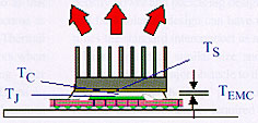
In the majority of applications involving plastic surface-mount packages, most of the heat generated by integrated circuits will flow to the printed circuit board (PCB) by way of the package leads and then to
In higher-power applications it is often necessary to attach a heat sink to the top of the package to keep the junction temperature of the chip within specified limits. The presence of a sufficiently large heat sink can cause the heat flow path out of the package top to become dominant.
In this situation, the temperature of the junction (active circuitry on top of the die) will be determined by the thermal resistances comprising the primary heat flow path:
- * Between the junction and the case (top of the package), namely
* The thermal resistance between the heat sink and the air, SA
JC is determined experimentally by the application of the following equation, in the form of a standard thermal resistance calculation:
where TJ and TC are the temperatures of the junction and the case, respectively, and PJC is the actual power flowing between the junction and the case. Experiments designed to measure JC are usually configured to force nearly 100% of the heat out of either the top or the bottom surface of the package, allowing the total power dissipated in the die to be used in the denominator of this equation.A conservative estimate of
JC for an IC package configured with epoxy molding compound (EMC) above the die is obtained by assuming 1-D heat flow from the die to the surface of the package:
where tEMC and KEMC are the thickness and thermal conductivity of the EMC layer above the die, respectively, and ADie is the area of the die. Putting in typical values of these three quantities into the above equation, one obtains: JC = 0.54 mm/(104 mm2 x 0.7 x 10-3 W/mm-K) = 7.4 °C/W.A conservative estimate of the difference between junction temperature and the ambient air can be obtained by use of the following equation:
 |
where P is the total power dissipated in the package, CS is calculated assuming the 1-D heat flow and
SA)` is obtained from the heat sink manufacturer. The sum of these three thermal resistances is lumped into a single resistance, the junction-to-air thermal resistance, or
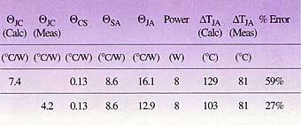
JA‘The following table shows a comparison of
TJA obtained using values of
JC determined using equation (2) and a measurement involving a 35 mm, 452 lead Plastic Ball Grid Array (PBGA) package. The values of ADie, tEMC and
EMC for this package correspond to those in the example above. The measured value of
JC is much less than the calculated value because of additional heat spreading by the package laminate, which contains 2 planes of 35 �m thick copper. This design leads to a heat flow to the top of the package over an area larger than that of the die. The heat sink used measured 50.5 mm x 50.5 mm x 10 mm. The interface material between the package and the heat sink was thermal grease, assumed to be 0.025 mm thick and to have a thermal conductivity of 2 W/mK. The measurements were performed in a PC graphics card environment with natural convection cooling.
 |
The calculated values of TJA, exceed the measured values by 59% and 27%, respectively. It is possible to perform a more accurate calculation of
JC. However, this would involve more complicated equations than equation (2). The accuracy of the calculation could be improved also by accounting for the additional heat flow path through the PCB. The presence of this parallel path causes a lower value of
JA than that due to heat flow through the heat sink alone. The method described here can be quite useful because of its simplicity. However, one must be aware of the very conservative nature of the calculation when interpreting the significance of the results.


