Various new advanced composite materials are now available, which provide great advantages over conventional materials for electronic packaging thermal control, including:
- Extremely high thermal conductivities (up to twice that of copper)
- Low, tailorable coefficients of thermal expansion
- Extremely high strength and stiffness
- Low densities
- Low cost, net shape fabrication processes
These characteristics provide the following benefits in packaging components:
- Significantly improved thermal performance
- Weight savings up to 80%
- Size reductions up to 65%
- Significant thermal stress reductions
- Design simplification
- Cost savings
The number of production applications is increasing steadily. Annual production rates for some commercial parts are in the range of hundreds of thousands.
This article provides an overview of advanced composites used in thermal management, including properties, applications and future trends. The focus is on materials having thermal conductivities at least as high as those of aluminum alloys.
Background
The continuing increase in packaging density necessitates materials with high thermal conductivities. In addition, to minimize thermal stresses that can cause component or solder failure, packaging materials should have coefficients of thermal expansion (CTEs) matching those of the materials to which they are attached, such as printed circuit boards (PCBs), ceramic substrates and semiconductors. Further, low density is desirable in many applications, including portable systems such as laptops, hand-held telephones and avionics. Reducing weight also minimizes potentially damaging stresses resulting from shock loads that can occur during shipping and from other causes. Of course, low cost is also a key consideration. Traditional materials used in electronic packaging do not meet all of these requirements. In response to this need, new composite materials have been, and are continuing to be developed [1-8].
Overview of Composite Materials
A composite material can be defined as two or more materials bonded together [2]. Composites are nothing new in electronic packaging. For example, glass fiber-reinforced polymers (GFRPs), which are polymer matrix composites, have been used in printed circuit boards (PCBs) for many years. Similarly, for many years, a variety of ceramic and metal particles have been added to polymers to reduce CTE and increase thermal conductivity, electrical conductivity, or both. These materials are particulate PMCs. New composites have been developed in recent years that provide unique combinations of properties that make them very attractive candidates for packaging applications.
The four key classes of composite materials are:
- Polymer Matrix Composites (PMCs)
- Metal Matrix Composites (MMCs)
- ceramic matrix composites (CMCs)
- Carbon/Carbon Composites (CCCs).
At this time, PMCs, MMCs, and CCCs are of interest for thermal management.
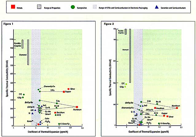
Figure 1, which plots thermal conductivity as a function of CTE for a variety of materials used in electronics, illustrates the limitations of traditional packaging materials. In order to minimize thermal stresses in packaging, it is generally necessary to match the CTEs of semiconductors like silicon and gallium arsenide and ceramic substrates, such as alumina, beryllia and aluminum nitride. These materials have CTEs in the range of 3-7 ppm/k (shaded area). In some cases it is necessary to attach to GFRP PCBs, which have CTEs in the range of 15 ppm/k. We see that aluminum and copper have good thermal conductivities, but CTEs that are higher than desired, especially for attachment to ceramics and semiconductors.
Traditional materials used to achieve low CTEs include “Kovar”, a nickel-iron alloy, and blends of copper and tungsten (Cu-W) or copper and molybdenum (Cu-Mo). We see that “Kovar” has a low thermal conductivity and a density much higher than that of aluminum. Cu-W and Cu-Mo, which are composites, rather than alloys, provide higher thermal conductivities than “Kovar”, but with significant weight and cost penalties.
Table 1, which is based on data from Reference 7, presents more detail about the properties of many of the materials in Figure 1. Note that fiber-reinforced composites tend to be anisotropic. Inplane values of thermal conductivity are shown.
| Table 1. Properties of selected electronic packaging materials [7] |
|||||
| Reinforcement | Matrix | Thermal Conductivity W/mK |
CTE ppm/k |
Modulus GPa |
Specific Gravity |
| – | Silicon | 150 | 4.1 | 2.3 | |
| – | Alumina | 20 | 6.7 | 380 | 3.9 |
| – | Aluminum | 120 | 23 | 69 | 2.7 |
| – | Copper | 400 | 17 | 117 | 8.9 |
| – | Epoxy | 1.7 | 54 | 3 | 1.2 |
| – | “Kovar” | 17 | 5.9 | 131 | 8.3 |
| Copper | Tungsten | 167 | 6.5 | 248 | 16.6 |
| Copper | Molybdenum | 184 | 7.0 | 282 | 10.0 |
| Beryllium | Aluminum | 210 | 13.9 | 179 | 2.1 |
| “Invar” | Silver | 153 | 6.5 | 110 | 8.8 |
| Carbon Fiber (K1100) | Epoxy | 300 | -1.1 | 186 | 1.8 |
| Carbon Fiber (K1100) | Copper | 400 | 6.5 | 158 | 7.2 |
| Carbon Fiber (K1100) | Aluminum | 290 | 6.5 | 131 | 2.5 |
| Discontinued Carbon Fiber (K1100) | Polymer | 20 | 4-7 | 30-50 | 1.6 |
| Carbon Fiber (K1100) | Carbon | 350 | -1.0 | 255 | 1.9 |
| Silicon Particle | Aluminum | 126-160 | 6.5-13.5 | 100-130 | 2.5-2.6 |
| SiC Particle | Aluminum | 170-220 | 6.2-7.3 | 225-265 | 3.0 |
| Beryllia Particle | Beryllium | 240 | 6.1 | 330 | 2.6 |
 |
Figure 1. Thermal conductivity as a function of coefficient of thermal expansion for materials used in electronic packaging [7].
Figure 2. Specific thermal conductivity (thermal conductivity divided by specific gravity) as a function of thermal expansion for materials used in electronic packaging [7].
There are a number of composite materials in Figure 1 which have CTEs in the desired range: silicon carbide particle-reinforced aluminum ([SiC]p/Al), carbon fiber-reinforced copper (C/Cu), carbon fiber-reinforced aluminum (C/Al), diamond particle-reinforced copper ([Diamond]p/Cu), and beryllia particle-reinforced beryllium ([BeO]p/Be). We observe a number of other materials which have high thermal conductivities, but which lie outside the shaded area. In addition to silver, aluminum and copper, they include pyrolitic graphite, carbon/carbon (C/C) composites, carbon fiber-reinforced epoxy (C/Ep) and, of course, diamond. The carbon fibers represented in Figure 1 are thermally conductive pitch-based materials that have nominal thermal conductivities as high as 1100 W/m K.
To compare packaging materials in applications for which both thermal conductivity and density are important, a useful figure of merit is specific thermal conductivity, which we define as thermal conductivity divided by density (for simplicity, we use specific gravity, which is dimensionless). Materials with high specific thermal conductivities are desirable in weight critical applications. Figure 2 presents specific thermal conductivity as a function of CTE for packaging materials. We observe that the specific thermal conductivities of traditional low-CTE packaging materials like “Kovar”, Cu-W and Cu-Mo are very low. However, the low densities of many composites, combined with their high thermal conductivities enhance their relative position. In fact, the specific thermal conductivities of some composites are more than an order of magnitude greater than those of “Kovar”, Cu-W and Cu-Mo.
There is a rule of thumb, which says that improving a critical property by an order of magnitude produces revolutionary technological change. It is not surprising, therefore, that composites are making significant inroads in electronic packaging.
A key advantage of some composites is that they are made by processes that produce parts having the final desired shape (net shape processes) or which require only a small amount of machining (near-net shape processes). Minimizing machining enhances the cost effectiveness of these materials. This is particularly true for silicon carbide particle-reinforced aluminum, often called Al/SiC, which is one of the most important of the new composite packaging materials and for carbon fiber-reinforced polymers, such as C/Ep. Another feature of a key process used to make Al/SiC, pressure infiltration casting, is that it allows direct incorporation of ceramic substrates, feed-throughs and seal rings [8]. Substrates are usually attached with a braze, solder or adhesive material. Elimination of this step reduces labor and also improves thermal performance because attachment materials typically have relatively low thermal conductivities.
Applications
Composites are now being used in important commercial and aerospace electronic packaging applications. Annual production for some parts is in the hundreds of thousands. Components include: carriers; lids for computer central processor units, complex hermetic microwave packages (modules); power semiconductor packages; solid and flow-through liquid cooled PCB cold plates (thermal planes), pin-fin heat sinks, thermal straps, enclosures and support structures [1, 3-7]. The key composite packaging materials at this time are Al/SiC and high conductivity carbon fiber-reinforced polymers.
The composite components cited in the previous paragraph are being used in numerous commercial and aerospace products, including: electric vehicles, motor controllers, cellular telephone base stations, laptop computers, high end cellular telephone handsets, and aircraft and spacecraft microwave antennas and power supply subsystems.
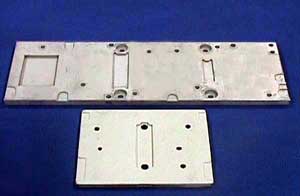
Two examples demonstrate the advantages of Al/SiC. Figure 3 shows two Al/SiC net shape carrier plates. The larger one duplicates the original that was machined from copper. In the original design, components were mounted on a number of small alumina substrates to minimize thermal stresses. Use of Al/SiC allowed direct attachment, improving thermal performance, and, allowing a reduction in carrier plate size of about 65%. Taking into account the lower density, the total weight savings is about 85%.
 |
Figure 3. Net shape Al/SiC carrier plates. Plate in the foreground reduces size by 65% and weight by 85% over the machined copper incumbent design. (Courtesy Ceramics Process Systems).
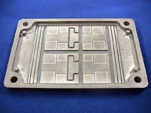
Figure 4 shows an Al/SiC IGBT package base in which an aluminum nitride substrate is incorporated directly during the aluminum infiltration process, eliminating the need for a separate soldering step and improving thermal performance because of the relatively high thermal resistance of solder layers.
 |
Figure 4. Net shape Al/SiC IGBT base plate. Aluminum nitride substrate is incorporated into the package during the aluminum infiltration process. (Courtesy Ceramics Process Systems).
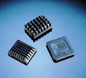
As mentioned earlier, the other key composite packaging materials at this time are PMCs reinforced with continuous and discontinuous thermally conductive carbon fibers. These materials have been used in production pin-fin heat sinks (discontinuous fibers) and PCB cold plates (continuous fibers). Figure 5 shows an array of developmental components made by net shape processes, including pin-fin heat sinks and computer central processor unit covers, all of which are reinforced with discontinuous fibers.
 |
Figure 5. Developmental carbon fiber-reinforced polymer pin-fin heat sinks and computer central processor unit covers. (Courtesy Bryte Technologies).
Cost Considerations
Cost is a complex issue, depending on the amounts and costs of constituents and processes, as well as part complexity, production run size, total annual production and maturity of the technology. A further complication is that costs and prices are typically proprietary and competition sensitive.
In considering cost, we also have to consider that advanced composites have only been in production for a relatively short time. History has shown that the cost of new materials typically decreases significantly with increasing volume. For example, standard modulus carbon fibers that cost $1000/lb in the U.S. when they were first introduced in the early 1970s are now available for $8/lb, and are projected to drop to $5/lb next year.
If we consider the current leading packaging composite, Al/SiC, we find that the constituents are very inexpensive; aluminum is about $1/lb and SiC particles, which are obtained from the commercial abrasives industry, sell for about $2/lb in large quantities. The issue, then, is the cost of the processes used to produce the component in its final form. We note that there are a number of very different processes used to make Al/SiC. At this time, all we can say is that the success of Al/SiC in commercial products like telephone base stations, laptop computers and power semiconductor modules demonstrates that they can be cost effective in some applications.
Future Trends
It is clear that packaging density and device power levels will continue to increase, as will the drives to reduce weight, size and cost. The result is a continuing need for improved thermal management materials having high thermal conductivities, low, tailorable CTEs and low-densities. These objectives can only be achieved through composites technology.
We are in the early stages the development of composite packaging materials. In the future, we will see improved materials in all classes, including PMCs, MMCs, CCCs and CMCs. Increasing production volumes and improved processes will reduce costs, making composites more competitive. This will lead to increasing use in new applications.
Acknowledgement
Figures 1-2 and the data in Table 1 and were taken from Reference 7, and appear courtesy of John Wiley and Sons, Inc.
References
1. C. Zweben, “Overview of Metal Matrix Composites for Electronic Packaging and Thermal Management”, JOM, July 1992.
2. Kelly, Concise Encyclopedia of Composite Materials, Pergamon Press, Oxford, 1988.
3. C. Thaw, J. Zemany and C. Zweben, “Metal Matrix Composites for Microwave Packaging Components”, Electronic Packaging and Production, August 1987, pp. 27-29.
4. C. Zweben and K.A. Schmidt, “Advanced Composite Packaging Materials”, Electronic Materials Handbook, ASM International, Materials Park, Ohio, 1989.
5. M. DiNardo, J. Kreitz and C. Zweben, “Lightweight Composite Electronics Enclosure for High Stress and Temperature Environments”, Proceedings, 35th International SAMPE Symposium and Exhibition, Anaheim, California, April 1990.
6. C. Zweben, “The Future of Advanced Composite Electronic Packaging”, Materials for Electronic Packaging, D. D. L. Chung, Ed. Butterworth-Heinemann, Oxford, 1995.
7. C. Zweben, “Composite Materials And Mechanical Design”, MECHANICAL ENGINEERS’ HANDBOOK, Second Edition, Myer Kutz, Ed, John Wiley & Sons, Inc., New York, 1998 (In Press).
8. M. Occhionero, R. A. Hay, R. W. Adams, and K. P. Fennessy, “Cost-Effective Manufacturing of Aluminum Silicon Carbide (AlSiC) Electronic Packages”, IMAPS Advanced Packaging Materials Symposium, Braselton Georgia, March 1999.


