 |
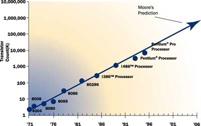
Figure 1. Transistor counts on Intel processors from inception to present superimposed on Moore’s prediction.
In his fascinating book, “Visions,” Michio Kaku [1] predicts a future driven by silicon and quantum computers. Based on the information we have today, it is intriguing to speculate how such a highly silicon-based society might function and evolve. Being a thermal engineer, I cannot help but to wonder how we are going to manage the thermal issues?
Will the electronics in home appliances require liquid cooling? Will cars feature special fins or extremities especially for cooling their onboard electronics? Will aircraft need cryogenically cooled electronic systems so they can fly safely? Alternatively, will the material and all other related technologies advance so that we can continue to use natural convection in air as the cooling mechanism? Or is it remotely possible our insatiable thirst for speed will eventually subside, allowing a return to cooler systems?
Almost from inception, power dissipation and its adverse impact on electronics has been a point of concern for the industry. Whether cooling vacuum tubes or sophisticated integrated circuits, an integral part of the design cycle has always been the consideration of power dissipation and consumption issues. Although the level of attention paid to thermal matters has been inconsistent at best as packaging and electronics technology has progressed from one era to the next, the reality is that the importance of thermal management to the ultimate success of new products has never diminished.
As the result of power dissipation, cooling technology has experienced a major evolution from liquid to air to, maybe in the future, cryogenics. However, the economics of cooling, coupled with the unmatched reliability of natural convection as a cooling system, continue to underscore the desire to cool systems and components with natural convection in air. On the other hand, the limitation of device temperature – the infamous junction temperature – has virtually stopped the use of natural convection in air. Thus, device-level power dissipation will remain a point of contention for equipment manufacturers and will impose larger challenges as the years pass.
Moore’s Law or Curse
For several decades Moore’s law has served as a beacon to predict device density and its subsequent power dissipation. The law, named after Intel founder Dr. Gordon Moore, states that semiconductor transistor density, and hence performance, doubles roughly every 18 months. Dr. Moore made his prediction in the 1970’s and history supports his conclusion, as shown in Figure 1 [2].
It is fascinating to observe how closely the microprocessor industry has followed Moore’s law. Incidentally, it is useful to note that this trend also applies to components other than microprocessors. Although little industry data is available, the evolution of CMOS technology clearly suggests the same trend.
In the 70s and 80s, Moore’s law served as a point of discussion – – and much disbelief. Many people never expected to see such densities. Moreover, once the transistor densities were converted into power dissipation the disbelief in Moore’s law was further amplified because the heat flux densities began to rival the space vehicle re-entry temperatures. In one simple Telecom example, we have seen the heat flux jump in the short span of ten years from 0.5 W/cm2 to more than 10 W/cm2 – a factor of 20! As a side note, the current lack of cooling technology and inaction on the thermal management industry to develop it further may be attributed directly to the disbelief of Moore’s law. So, when viewed from the thermal management standpoint, it appears that Moore’s law has been rather a curse.
Power Dissipation Projection
Gordon Moore’s insightful observation on device advancement has had a direct correlation with power dissipation. Figure 2 shows the power dissipation of some representative Intel microprocessors as a function of time, [3].
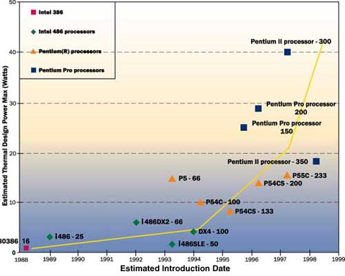 |
Figure 2. Time-line plot of Intel corporation microprocessor power dissipation.
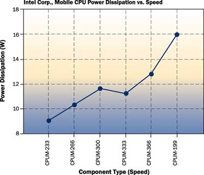
The scatter in data clearly suggests technology advancements to reduce power. But the overall trend is the exponential increase in power dissipation with time. This trend is not particular to one company’s technology. When we look at AMD Corporation, Figure 3, we see the identical trend when we plot power dissipation versus device frequency – reflective of time. Even when we look at more power-conscious electronics, such as portable systems, in Figure 4, we see the same trend shown in Figure 2.
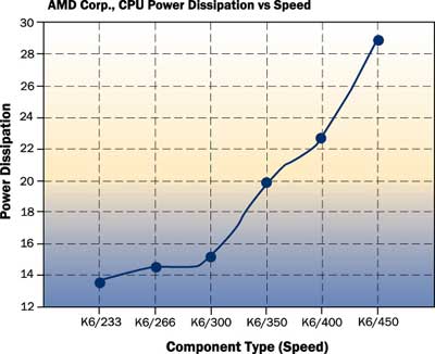 |
Figure 3. Power dissipation of the AMD Corp. K6 family of microprocessors as a function of time (clock sppeed reflects time history).
Figure 4. Power dissipation of the Intel Corp. family of mobile microprocessors as a function of time (clock speed reflects time history).
With the current device and manufacturing technologies, all industry beacons point to significant power increases with time. None of the plots displayed above indicates that power dissipation at the chip level – and subsequently at the system level – is declining or even reaching a plateau.
The Reason for Power Dissipation Increase
Two causal agents underlie this increase in power dissipation: speed and the number of gates on the silicon. Over the years, there has been much effort to reduce the size of the devices (transistors, diodes, etc.) on the silicon wafer. More than a decade ago, 1.5 micron (�m) appeared to be the limit and this caused much enthusiasm about the possibilities for this new technology. Today, by contrast, geometries down to 0.18 �m are gaining in popularity and soon to become the standard. The 0.18 �m device size, like its predecessors has created much excitement as chip designers contemplate “system-on-chip” products. Figure 5, illustrates Intel device technology as a function of time. The timeline chart clearly shows a rapid decline in part size as a function of time, and this trend shows no sign of reaching the asymptotic condition (plateau). If we define the lower size limit to be the atomic or molecular scale, it appears that the downward trend will continue accompanied by the challenge to develop production hardware capable of making parts that small (transistors, diodes, etc.).
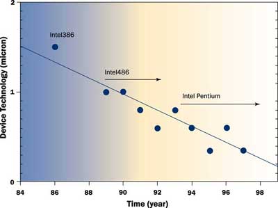 |
Figure 5. Intel device technology as a function of time.
It is interesting to consider what happens if we superimpose Figures 2 and 5. Though not plotted in this article, it is clear that as technology has shrunk part size, power dissipation – attributable to increases in speed – has continued to rise. Table 1 sheds some light on this process [4]. The table chronicles the number of gates used in a device and the power dissipation as the device technology advances. A number of salient points help us understand why power dissipation has increased and will continue to increase.
Foremost, we notice a ten-fold increase in the number of gates per device from 1995 to present. It is anticipated that this number will grow to 6-to-8 million by the 2001. In the past four years, feature size has shrunk from 0.35 to 0.25 �m. Indeed, the latter is almost an industry norm and 0.18 �m is poised on the horizon. Similarly, voltage that activates the device has decreased from 3.3V in 1995 to 2.5V in 1999 and is likely to continue decreasing in the near future.
The most intriguing and perhaps confusing point involves power. Power consumption per gate has decreased dramatically from 0.64 to 0.15�W/Gate/MHz. Yet, overall power dissipation has risen dramatically for just about every component on the market. This phenomenon can be attributed to two factors: the increased number of devices on a die (gates/device) and speed. As indicated in Table 1, the industry in general is placing more parts on chips. Also, processing speed has accelerated dramatically as evident in the CPU industry (See Figures 1 through 4).
| Year | No. Gates/Device |
Feature Size (�m) |
Voltage | Power (uW/Gate/MHz) |
| 1995 | 300k | .035 | 3.3V | 0.64 |
| 1997 | 1m | 0.25 | 3.0V | 0.27 |
| 1999 | 3m | 0.25 | 2.5V | 0.15 |
Table 1. The Gate Count and Date Power Trend for Standard Devices [4].
A simple calculation demonstrates the effect of speed on power dissipation. Suppose we have two devices, 500 and 600 MHz, respectively, with each containing five million parts (gates). If we use today’s technology, the power will be 0.15 . Performing a simple algebraic calculation, we can determine that the power dissipation in such a device is 375 W and 450 W for the 500 and 600 MHz dies, respectively. Such power dissipation in a spatially constrained environment is, at times, beyond imagination.
To gain an appreciation for these power levels and their impact, let us compare a 100W light bulb with a ball grid array (BGA) device that dissipates 25 W(Table 2).
| Light Bulb | BGA Package | |
| Power dissipation | 100W | 25W |
| Surface area | 106cm2 (bulb surface area) |
1.96 cm2 die area |
| Heat flux | 0.9 W/cm2 | 12.75 W/cm2 |
Table 2. Comparison of Heat Flux between a Light Bulb and a BGA Package.
The heat flux of a light bulb is approximately 13 times less than that of the BGA. Furthermore, the light bulb can dissipate heat through an entire room, whereas the BGA is confined to the small space provided between two PCBs. Certainly, we do not want to touch a light bulb that has been on for a while. Thus you can imagine the potential temperature of a device residing on a PCB with such power densities. We can therefore conclude that the combination of higher speed, number of parts on the die and spatial constraints collectively result in power dissipation and a thermal management situation that is challenging, if not impossible, to meet with today’s technology and design constraints, e.g., T j,max = 125°C.
Source of Power in CMOS Technology
Across a variety of electronics industry segments, device power dissipation has become the important player in ASIC design. A successful chip design requires low power consideration, and determination of the locations (spots) on the die where power dissipation occurs. The design objective is to minimize device junction temperature because temperature directly impacts die performance (speed, sinking and sourcing capability). Therefore, understanding the source of the power may shed some light onto what the future may offer and may perhaps expose the limits that currently confronts the designer.
“Today’s advanced IC designs contain millions of transistors and run at clock frequencies approaching 1 GHz. These designs, which combine analog circuitry, memories, standard cell logic, and custom processor cores, are truly systems on a chip. Semiconductor technology at 350 nm is in volume production around the world, with the road map extending to ever-smaller geometry. As device dimensions continue to shrink in this deep-submicron or nanometer realm, the physical characteristics of semiconductor devices become increasingly complex. Designers are faced with new challenges for accurately predicting circuit performance. In addition, as both the clock speed and the number of devices on the chip increase, power consumption is emerging as a major concern. For portable applications, long battery life is extremely important to enhance the competitiveness of the end product. For non-portable applications, excessive heat generated by high power consumption can lead to device reliability problems” [5].
Irrespective of application, three components are attributed to power dissipation in digital CMOS circuits:
1. Dynamic switching current is used in charging and discharging circuit load capacitance, which is composed of gate and interconnect capacitance. The greater this dynamic switching current is, the faster you can charge and discharge capacitive loads, and your circuit will perform better.
2. Short-circuit current is that which flows between the power supplies for a period of time when both p- and n-channel devices are on during signal transitions at the inputs of logic gates. Short-circuit current increases with slower signal transition times.
3. Leakage, or DC standby current, occurs because of sub-threshold conduction in MOSFETs. This current is independent of switching activity, but is a strong function of power supply voltage and operating temperature. Leakage current is usually small, but in large ultra low power designs (such as memories), it can represent the majority of the standby power consumed by the device” [5].
Switching power is the dominant source of power drain on a CMOS chip. Each time a transistor switches state, it either pumps charge into a capacitor (the load), or drains the capacitor to ground. In a full cycle, charge is taken from the rail and pumped to ground. This produces a current, which, multiplied by the rail voltage, equals power. If the transistor does not switch as often, less charge moves and the power is lower. This is why limiting the activity of transistors is an excellent way to limit power.
There are also other kinds of power to worry about, specifically, static power and leakage power. Static power, as the name implies, is constant with activity. Many analog circuits appear to have static power, since they are continuously “on” and drain power at a relatively stable rate. Bipolar circuits draw a constant current, as well as a switching current [6].
The power problem for the CMOS devices did not surprise IC foundries, and they have been aggressively lowering their voltages (Table 1). But for anyone who has watched power consumption grow in microprocessors even as voltage is lowered, it is clear that simply lowering voltages is not enough (Figures 1 through 4).
From the above discussion, it is clear that significant work lies ahead for reducing and managing power dissipation in CMOS devices. With the market desire to shrink size and put systems on chips, advances in circuit design and materials are clearly required for managing this situation, since neither speed nor size is helping power reduction. Otherwise, Moore’s law continues to be applicable and the power trends observed here will continue to apply.
Role of Technology
The electronics industry has tried to rely on technology to save it from the impact of power dissipation. Migration from vacuum tubes to silicon and from Bipolar to CMOS appears not to have solved the problem. Figure 6 chronicles the role of cooling and circuit technology in the past several decades.
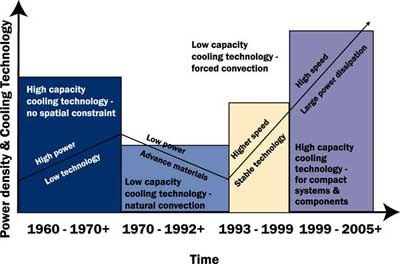 |
Figure 6. Thermal and circuit technology trends over the several decades.
In the sixties, the power consumption/dissipation of early electronics was high. Since there was no obvious spatial constraint, providing high capacity cooling in large rooms was the norm. Nevertheless, the limitations in both speed and size forced advances in circuit design and materials that reduced power dramatically and subsequently required low cooling technology and natural convection in air. Only a few exotic or high-speed computers required either air conditioning or forced convection cooling by air. This comfort zone continued to dominate for many years and created a false sense of security that the issue of heat may have been overcome. This was further amplified by the aggressive introduction of CMOS technology that continues to replace Bipolar technology [7]. The comparison between the two technologies, depicted in Figure 7, clearly shows that the new technology bought the industry only 10 years. As shown, CMOS and Bipolar technologies have paralleled each other with a 10 year time shift.
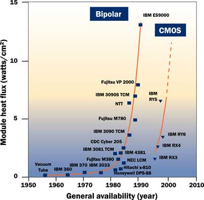 |
Figure 7. Power dissipation trends, comparison of Bipolar and CMOS technologies, [7].
Only a handful of companies involved in high-speed computing and military/space applications have proven exceptions to the norm. The rest of the industry viewed thermal management issues as simply a matter of adding heat sinks!!! From early nineties, with the popularity of and easy access to personal computers and, subsequently, the Internet, a paradigm shift occurred. This was the issue of speed. Mass access to electronics and consumers expecting instantaneous response (like turning a light on) forced many companies to provide higher speed systems and services. Speed requirements necessitated smaller devices and systems. Consequently, power dissipation has become a major challenge and its management is a critical technology in the electronics industry. Moreover, there are no indications of circuit speed decreasing or of space requirements changing. To address current and future issues, technological advancement is likely the only savior; that is the introduction of new materials, new cooling technologies and a paradigm shift in cooling technology concepts and modes of implementation.
A look at the Future
How do we define the future? This is rather a challenging task. For the purpose of this discussion, let us define it both near term (3 to 10 years) and long term (anything over 10 years).
Based on what we know to date, making some projections for the next 5 to 10 years is fairly straightforward. If there are no step changes in technology implementation – and there is no data to support that such a shift will occur – it is apparent that power dissipation will be a major bottleneck across the industry. For the near future, all data presented here and elsewhere points to die level heat fluxes of 40 to 50 W/cm2 as the norm, not the exception. Barring specialized electronics that may exceed these levels (ultra-speed computers and space/military applications), this implies board power dissipation of several hundred watts and systems of several kilowatts. Furthermore, there are no indications that speed is decreasing or that the industry is stepping away from the system-on-chip concept. The combination of speed, compactness and system features will push power dissipation and its management to the limit.
The far future is difficult to predict. Much interesting work, taking place within the industrial and government laboratories, may provide a shift sought by the electronics industry. Some of these technologies include silicon germanium (SiGe) and hold a promise of freeing the industry from Moore’s law! Another technology involves amorphous computing , where tiny self-organizing computers are suspended in an electrolytic solution. Other exotic technologies embrace computing and signal processing based on DNA, Optical and Quantum machines. These technologies will revolutionize the whole concept of signal processing and computing. The possibilities are endless, and the obstacles to building tangible applications with these technologies are daunting.
Will the future technology eliminate problems associated with power dissipation? The honest answer is “I do not know”. At this time, we cannot say whether SiGe will “repeal” Moore’s law, or, like CMOS, simply buy us time. The exotic concepts that are vigorously being researched – DNA, Optical, and the like – are just too fresh on the drawing board to fully comprehend their implications for practical development.
The reality is the near future problems – year 2005, when the exotic solutions are neither formed nor yet introduced. All data suggests that device power dissipation will increase exponentially with time. Moreover, considering the anticipated heat fluxes, thermal management of such systems is not possible with today’s technology and design constraints. It is evident that the electronics industry has been unable to stem or control power dissipation growth. Thus, to produce functional systems that can meet consumer expectations, we must accept a paradigm shift. Either we must accept slower systems with larger volumes, or move towards thermal management solutions that depart dramatically from what is conventionally implemented today.
References:
1. Kaku, M. “Visions- How Science Will Revolutionize the 21st Century,” Anchor Book, 1997.
2. Colwell, R. “CPU Power Challenges 1999”, ISPLED ’99
3. Personal communication with R. Colewell, Intel Corporation.
4. Lucent Technology Microelectronics Data Book
5. Ruby, W. M. “Managing Power Dissipation in System-on-a-Chip Designs” Web publication.
6. Frenkil, G. “Controlling Power Dissipation in Submicron IC’s,” Web publication.
7. Chu, R.C., Simons, R.E., and Chrysler, G.M., “Experimental Investigation of an Enhanced Thermosyphon Heat Loop for Cooling of a High Performance Electronics Module,” Proceedings of the 15th IEEE Semiconductor Thermal Measurement and Management Symposium,” pp.1-9, 1999.

