Improving thermal performance of electronic components is very challenging due to the increasing power density and decreasing module sizes. The design trade off between electrical and mechanical characteristics and the cost of manufacturing MCM products requires innovative solutions to improve device thermal performance.
The primary cooling path in portable electronics serves to provide a low resistance path from the heat source to the system card and to spread the heat in its respective conductive layers. Numerous design techniques are implemented to achieve the optimal thermal performance of MCMs [1]. However, conventional heat removal paths do not provide a sufficient thermal solution for power amplifier (PA) MCMs if they are to have a higher duty cycle or higher output power. The authors therefore pursued a system level cooling design by performing transient thermal analysis and employing micro heat pipes.
In the case of high-speed power input typical of PAs, detailed transient thermal analysis is required to understand system behavior [2-4]. The formulation of a system’s transient response to a pulsed input power is discussed separately [2]. Additionally, the use of micro heat pipes as system level cooling solutions used in portable electronic products, such as laptop computers, has been previously shown [5-9]. In this article, the authors demonstrate the use of micro heat pipes to cool PA MCMs in a cellular phone application.
Test Vehicle Structure
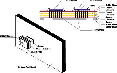
As a test vehicle, the authors used a global system for mobile communication (GSM) base-band power amplifier multi chip module. A four layer 100 sq. mm laminate substrate serves to interconnect two active devices: one GaAs and one silicon, along with more than 20 discrete ceramic components. The active devices measure 1.10 mm x 1.60 mm for the GaAs die and 1.10 mm x 1.10 mm for the silicon die. The package incorporates land grid peripheral terminals with a large central pad in the middle. It is surface mounted at the lower left corner of a 40 mm x 80 mm six layer test board.
The authors selected the test board characteristics and the location of the MCM to represent a card that is typically used in a cellular phone application. A host of thermal vias, all shorted to the ground plane, transfers heat from the top surface of the die to the external test board. Figure 1 shows the test vehicle and the package internal structure.
 |
Numerical Analysis
Package thermal performance was characterized in both component level and system levels. Component level analysis was required to capture the effect of package internal thermal design, as system level analysis could not capture this data due to the design complexity, high-speed power input and existence of localized heat sources.
Component Level Analysis
To characterize package thermal performance at a component level, the authors used a commercially available finite element analysis (FEA) tool (ANSYS 5.5 FEA software). A sub modeling analysis technique was employed for this analysis.
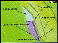 |
Figure 2. Component level finite element model. Some parts of the model have been removed for clarity.
Figure 2 shows the global model with some parts removed for clarity. The simulated model incorporated a detailed internal structure of the package, including copper layers, exposed die attach pad and thermal vias. Necessary boundary conditions were applied on the surfaces of the test board and the package [10]. Two different cases were simulated. In the first case, both devices were covered with glob top material; in the second case, the glob top was removed.
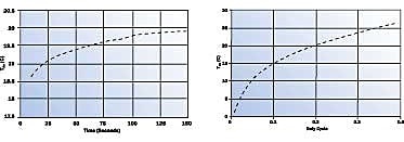 |
Figure 3. T DC (mean value of maximum junction temperature rise) as a function of time and T Ac (pulsed component of maximum junction temperature rise) as a function of duty cycle.
Due to the high-speed input power, the authors also conducted a transient thermal analysis. Figure 3 shows the mean value of maximum junction temperature rise over the ambient as a function of time, as well as its pulsed component as a function of power operating duty cycle. Both graphs reflect a power value of 2.50 Watts with a duty cycle of 1/8 and a package without glob top. Figure 4 shows the temperature distribution within the package.
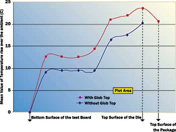 |
Figure 4. Temperature distribution within the package along an axis perpendicular to the substrate plane.
Next, to evaluate the heat spreading effects within the GaAs device, the authors performed a very fine meshed sub-modeling analysis. Global modeling analysis results provided the proper boundary conditions for the sub modeling efforts. The sub-modeling was done to analyze the effect of back-side vias and localized heat sources on the top metal layers of the device. Back-side vias are blind-via structures formed in a thinned GaAs wafer.
Figure 5 shows the temperature distribution within the GaAs die. The analysis results indicate an almost 8.50°C temperature difference between the top and bottom surface of the die if backside vias are used. The back-side vias prevent heat spreading and transfer the heat directly from the top surface of the die to the bottom side of the die. If no back-side vias were used, there would be an approximately 17.50°C temperature difference between the top and bottom surface of the GaAs die.
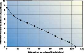 |
Figure 5. Temperature distribution within the GaAs device.
System Level Analysis
To predict the overall package thermal performance in a real application, the authors needed to perform a system level analysis. This was done using a computational fluid dynamics (CFD) tool (FLOTHERM). To ensure that both system level and component level modeling efforts would follow the same accuracy, a numerical wind tunnel (NWT) was used. The NWT provided the same performance conditions for both finite element and CFD analyses. An NWT was also used to create a compact system level model for the MCM.
The analysis results show an additional 6.2°C junction temperature rise over ambient compared to the still air case. This is due to the enclosed environment of the cellular phone. For the simulation, a maximum power dissipation of 2.50 Watts with a duty cycle of 1/8 was considered.
The system was redesigned to achieve a better thermal performance by using a micro heat pipe. The micro heat pipe transfers heat from the MCM-to-board interface partially to the cellular phone body and the rest to the antenna where it is transferred to the outside world through a mixed convection-radiation mechanism.
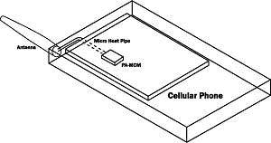 |
Figure 6. Using micro heat pipe in a cellular phone application.
The MCM with an exposed large center pad is soldered to a system card. A micro heat pipe is then soldered to the bottom of the system card. The other side of the heat pipe connects to the antenna as shown in Figure 6. A 2-mm diameter heat pipe (provided by Thermacore Inc. with the required thermal characteristics) was used in the analysis.
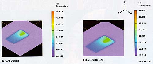 |
Figure 7. System level analysis results.
Figure 7 shows the system level CFD analysis results for the current design as well as for the enhanced system. The results show an almost 26% decrease in the maximum junction temperature rise over the ambient when a micro heat pipe is used.
Experimental Analysis
An extensive series of experiments was performed to validate the numerical analysis results at both the component and system levels. As validation of the numerical analysis results at the component level, the authors used a high speed IR camera, capable of up to 2000 images per second, to measure the junction temperature during the device operation.
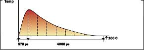 |
Figure 8. High speed thermal measurement.
Figure 8 shows typical captured images during a time period of 4630 microseconds after the system reached a steady state condition. The time scale was set up to capture a minimum of one frame in each time zone of 578 microseconds (i.e., 1/8 duty cycle). Figure 9 shows the experimental results for maximum junction temperature rise over ambient in the steady state condition. As seen, the experimentally confirmed results show an almost 26% improvement in MCM package thermal performance by using a micro-heat pipe in the proposed implementation.
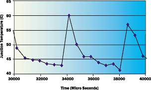 |
Figure 9. Maximum junction temperature rise over the ambient at the steady state condition.
Conclusions
To evaluate thermal performance of a high-speed RF power amplifier multi chip module in a cellular phone environment, device level, component level and system level analyses were conducted The use of micro heat pipes introduced an extended heat removal path. Analysis results, verified experimentally, showed an almost 26% decrease in maximum junction temperature rise of the MCM. This promises to enhance the electrical and mechanical reliability of the power amplifier MCMs and raises the possibility of operating at a higher duty cycle value.
Along with evaluating the new system, experimentally validated models were developed for design performance optimization. The calibrated models are being used to optimize the thermal performance of the Conexant Multi Chip Modules in relevant environments.
References
1.H. Hashemi and C. Davidson, ” Design for Manufacturing of RF MCM-L,” to be published in Interpack 1999 Proceedings, June 1999.
2.A. Langari and H. Hashemi, ” Thermal Transient Analysis of a Power Amplifier Multi Chip Module ” International Symposium of Micro Electronic- IMPAS 98, pp. 844-849, Nov. 1-4, 1998.
3.Hanilatha, V., Da-Guang Liu, Nakhala. M. S., Qi-Jun Zhang, ” Nonlinear transient thermal analysis using circuit simulation techniques, ” Proceeding of the 1995 Electronic Components and Technology Conference (ECTC), pp. 879-883, May 21-24, 1995.
4.Raghavan. J., Rahman, M. M., “Transient response of discrete heat sources on a conducting board in the presence of cross flow mixed convection,” Proceeding of Energy Conversion Engineering Conference (IECEC) pp. 1384-1389, Vol. 2, Aug. 11-16, 1996.
5.Ortega A., lall, B.S., Chicci, J. Aghazadeh, M. and Kiang B. ” Heat Transfer in low aspect ratio horizontal enclosure for laptop computer application” Semiconductor Thermal Measurement and Management Symposium – SEMI-THERM, pp. 42-49, Feb. 2-4, 19963.
6.Xie, H. Aghazadeh, M. Lui W., and Haley, K. ” Thermal Solutions to Pentium Processors in TCP in notebooks and sub-notebook” Proceeding of the 1995 Electronic Components and Technology Conference (ECTC), pp. 201-210, May 21-24, 1995.
7.Iswannath R.Ali I. A. ” Thermal modeling of high performance packages in portable computers” Proceeding of the 1995 Electronic Components and Technology Conference (ECTC), pp. 1122-1133, May 21-24, 1995.
8.Xie, H. Aghazadeh, M. and Toth. J. ” The use of heat pipes in the cooling of portables with high power packages – A case study with the Pentium processor- based notebooks and sub-notebooks. ” Proceeding of the 1995 Electronic Components and Technology Conference (ECTC), pp. 906-913, May 21-24, 1995.
9.Marongiu M. J, Kusha B. Fallon, G. S., and Watwe, A. A. ” Enhancement of multi chip modules (MCMs) cooling incorporating micro-heat pipes and other high thermal conductivity materials into mechanical micro channel heat sinks”, Proceeding of the 1995 Electronic Components and Technology Conference (ECTC), pp. 1122-1133, May 21-24, 1998.
10.Incropera, F., and Dewitt, P., ” Fundamentals of Heat Transfer” 3rd edition, John Wiley & Sons, 1990, New York, NY.


