In recent issues, this column has dealt with the use of a number of thermal metrics to calculate the junction temperature of integrated circuits under various conditions. These metrics explored were ![]() JA,
JA, ![]() JC, and
JC, and ![]() JT. To summarize the uses of these metrics:
JT. To summarize the uses of these metrics:
 JA represents the junction-to-air thermal resistance for a package tested in an industry-standard test environment. It is useful in determining changes in thermal performance due to design changes and for ranking package thermal performance.
  JA is of limited value in predicting the junction temperature in an application.
 JC, the junction-to-case thermal resistance, is useful in predicting the junction temperature when a package has a heat-sink mounted on top of it.
 JT, the junction-to-top of package thermal characterization parameter, is used to determine the junction temperature of a chip in an existing system from a measurement of the temperature on the top of the package.
None of these metrics is useful in predicting the junction temperature in a semiconductor package without a heat sink in an actual system. When there is no heat sink, the primary heat flow path for a surface-mounted package is typically though the PCB. Hence, this situation requires a thermal metric relating the junction and the board temperatures.
The recently specified ![]() JB thermal resistance metric [1,2] is measured under conditions in which nearly all of the heat is flowing to the board. It is useful in the analysis of actual systems when it is used as a component in a thermal resistor network defining the other heat flow paths.The thermal characterization parameter
JB thermal resistance metric [1,2] is measured under conditions in which nearly all of the heat is flowing to the board. It is useful in the analysis of actual systems when it is used as a component in a thermal resistor network defining the other heat flow paths.The thermal characterization parameter ![]() JB [1,3] is measured under conditions more typical of actual applications — namely with most of the heat flowing through the board, but a non-negligible portion of it flowing from the top of the package to the air. Hence, it is a stand-alone parameter that can be quite useful in predicting the junction temperature from a measurement of the board temperature.
JB [1,3] is measured under conditions more typical of actual applications — namely with most of the heat flowing through the board, but a non-negligible portion of it flowing from the top of the package to the air. Hence, it is a stand-alone parameter that can be quite useful in predicting the junction temperature from a measurement of the board temperature.
![]() JB is defined as
JB is defined as![]() JB = TJ – TB / Pwhere the board temperature, TB, is measured just beyond the package edge, along its centerline, preferably by soldering a type T thermocouple to the appropriate trace on the board. P represents the total power dissipated on the device.
JB = TJ – TB / Pwhere the board temperature, TB, is measured just beyond the package edge, along its centerline, preferably by soldering a type T thermocouple to the appropriate trace on the board. P represents the total power dissipated on the device.
The value of ![]() JB for a particular package depends upon many factors in the package design. These factors will not be explored here. However, some insight into to behavior of
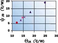
JB for a particular package depends upon many factors in the package design. These factors will not be explored here. However, some insight into to behavior of ![]() JB for a popular package format can be derived from examining the graph top right. This graph demonstrates the relationship between
JB for a popular package format can be derived from examining the graph top right. This graph demonstrates the relationship between ![]() JB and
JB and ![]() JA, a much more widely known parameter, for a family of 35 mm PBGA packages of varying thermal performance.The graph indicates that, for this particular group of packages
JA, a much more widely known parameter, for a family of 35 mm PBGA packages of varying thermal performance.The graph indicates that, for this particular group of packages ![]() JA, varies from 12 to 25°C/W.
JA, varies from 12 to 25°C/W. ![]() JB has a linear relationship with respect to
JB has a linear relationship with respect to ![]() JA and varies between 5 and 19°C/W. This behavior is consistent with the fact that the dominant heat flow path is from the junction to the board to the air. Since
JA and varies between 5 and 19°C/W. This behavior is consistent with the fact that the dominant heat flow path is from the junction to the board to the air. Since ![]() JB characterizes the thermal efficiency of this path, a reduction in
JB characterizes the thermal efficiency of this path, a reduction in ![]() JB is manifested as an equivalent reduction in
JB is manifested as an equivalent reduction in ![]() JA.
JA.
 |
Figure 1. ![]() JB versus
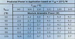
JB versus ![]() JA for a family of 35 mm PBGA packages of varying construciton. Packages mounted to JEDEC-standard test board. Natural convection conditions.The following Table illustrates how
JA for a family of 35 mm PBGA packages of varying construciton. Packages mounted to JEDEC-standard test board. Natural convection conditions.The following Table illustrates how ![]() JB can be used to predict the maximum power for a device, consistent with the maximum allowable junction temperature and the board temperature. In this hypothetical example
JB can be used to predict the maximum power for a device, consistent with the maximum allowable junction temperature and the board temperature. In this hypothetical example ![]() JB equals 15°C/W.
JB equals 15°C/W.
This table makes it very clear that the maximum power possible in a package depends on three factors: TJ,Max, which is specified by the semiconductor producer; TB, which is controlled by the system house; and ![]() JB, which is determined by the chip and package design.It is rare for the semiconductor producer or the package provider to know TB. However, such a table can be the start of a three-way dialog in which the impact of the board temperature on the maximum allowable power is defined. This, in turn, can help facilitate informed decisions regarding cost/performance tradeoffs between packaging choices and system design.
JB, which is determined by the chip and package design.It is rare for the semiconductor producer or the package provider to know TB. However, such a table can be the start of a three-way dialog in which the impact of the board temperature on the maximum allowable power is defined. This, in turn, can help facilitate informed decisions regarding cost/performance tradeoffs between packaging choices and system design.
References
1. Bennet Joiner, “Use of Junction-to-Board Thermal Resistance in Predictive Engineering,” Electronics Cooling Magazine, Vol.5, No. 1, (January, 1999), pp. 14-17.
2. JEDEC Standard, “Integrated Circuits Thermal Test Method Environmental Conditions – Junction-to_Board,” EIA/JESD51-8. [Available for downloading at www.jedec.org at no charge.]
3. JEDEC Standard, “Integrated Circuits Thermal Test Method Environmental Conditions – Forced Convection (Moving Air),” EIA/JESD51-6.


