Thermal test dies are among the major tools used in package thermal design qualification. They are usually simple chips, containing heaters and temperature sensors. The sensors measure the temperature on the chip surface as a result of the steady state powering or the time dependence of the temperature increase or decrease in case of transient qualification. From these data, the heat transfer properties of the package can be calculated, and thus various cooling conditions can be evaluated easily.
Thermal test dies are gaining increasing importance today in the thermal qualification of packages for several reasons. On one hand, the increased power density in today’s sophisticated new packages necessitates more careful design and more complex test tools for evaluation. On the other hand, there is a parallel development of thermal transient measurement tools, which can measure the temperature values at various locations simultaneously to provide data for calculating the chip-inside thermal transfer parameters. Consequently, more sophisticated, computer-controlled thermal test chips are appearing to support more complex measurements.
These new thermal test chips allow software-controlled selection of the location of the active sensors within the package, and software-controlled modification of the dissipation pattern of the chip. Such thermal test chips — if they are measured with appropriate testers and evaluated by sophisticated software — can deliver detailed data about the heat transfer properties within the chip itself and can also be used to qualify the die attach. Meanwhile, the old-fashioned, relatively simple thermal test dies remain in use too, mainly for static package qualification in the design phase.
Thermal test dies were originally used to determine Rth values of packages. In order to make the different measurements comparable, the thermal test dies must fulfill certain uniformity requirements. These were specified by various standards; for example, JEDEC JESD 51-4, SEMI G320-96, and MIL 883. Since the most widely used industrial standard today is JEDEC, it is worthwhile to briefly summarize what it prescribes for thermal test dies.
JEDEC Guidelines [1]
The major JEDEC requirement is to assure uniform heating on the chip surface. To achieve this, the standard prescribes that a minimum 85% of the chip area inside the bonding pads must be covered by evenly powered heating elements. A thermal test die must include the following elements:
- Heat source
- Thermal sensors
- Connecting pads
There is no strict prescription concerning the heater, however the standard does mention the resistor and transistor as two possibilities. Transistors prove more advantageous for use in transient measurements, but it is more difficult to obtain uniform dissipation with them. In the case of resistor dissipators, switching on and off is more problematic.
For sensing purposes, the standard mentions — but does not specifically prescribe — two possibilities: diodes and resistors. If one uses a forward biased diode, the change in the diode’s voltage is measured while the diode current is kept constant.
The other possibility is to use resistor temperature detectors (RTD), where the resistors are formed on one of the metal layers. The advantage of the RTD-based temperature sensor is much higher linearity over a much broader temperature range [2]. In the case of RTD sensors, the 4-wire connection is recommended. The resistor may be either a spiral or meander shape.
When using multiple thermal test dies in a package, each die must contain dissipator(s) and thermal sensor(s). In such cases, non-uniform dissipation of the different parts is allowed.
The following sizes are recommended for thermal test dies:
Chip thickness:
- 0.28, 0.375, 0.62 mm
Chip dimensions:
- Square: 2×2, 3×3, 4×4, 6×6, 9×9, 12×12, 15×15, 18×18, 24×24 mm
- Rectangular: 2×4, 4×6, 6×12, 9×18, 12×18, 12×24, 18×24 mm
Temperature sensors must be placed in proximity to the hot spot locations. In the case of a single-unit chip and uniform heating, this is presumably in the middle of the chip, so a sensor must be placed there. Additional sensors may be placed in a corner and in the middle of an edge for other purposes.
When a multiple-unit chip is used, one sensor should be placed at each unit center. A sensor must also be placed in one of the corners of each unit. It is necessary to provide a centrally-located sensor even when using an even numbered array of basic units. The sensors should be connected to four pads, with each pad no smaller than 0.1 mm. The heater and the sensor should not use common pads. It is also recommended that bonding pads, connected to the package in a manner similar to real applications, surround the entire chip.
It is interesting to consider how available test dies comply with these recommendations in terms of similarities and differences. The author has attempted to collect all available public information about test dies. Data are drawn from papers in scientific periodicals, Internet searches and information collected from die users. The most important features of these appear in the following sections of this article.
Main Characteristics of Thermal Test Dies
(identified by manufacturer name)
IBM
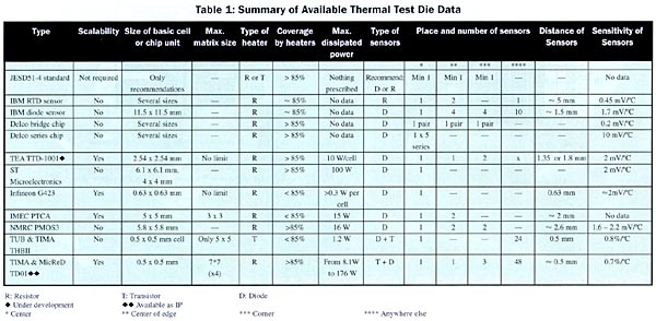
The IBM thermal test dies were presented in a paper at SEMITHERM in 1997 [2]. According to this paper, IBM has two different thermal test die families. In one of them the temperature sensor elements are pn junction diodes and in the other one they are RTDs. The goal of the authors, Claasen and Shaukatullah, was to present a comparative study of these two test vehicles. The authors found the RTD temperature sensors much more linear in the case of constant current than the diode sensors. For further data, see Table1.
Delco Electronics has developed two families of test chips for measuring thermal resistance. The chips are fabricated in different sizes to allow a choice that approximates active die sizes being produced. The so-called Bridge chip has two diodes and two resistors in a bridge configuration. The Temp chips go further by placing the diode legs of the circuit in three locations of each chip.
The other family of the Delco thermal test chips was designed for TAB packages. The so-called Series or TAB Temp chip has 52 bond sites, out of which eight are electrically active. Four of these are connected to the heating resistor and four to the sensing circuit. The sensing portion of the TAB Temp chips consists of five diodes, connected serially and located in the center of the die. Because of the serial connection, the temperature sensitivity increases up to 10 mV/C�. [3]
ST Microelectronics
The ST Microelectronics thermal test die is available in two sizes (6.1 x 6.1 mm and 4 x 4 mm). A die consists of one resistor (35 mm2 for the larger die; 15 mm2 for the smaller die) and one sensing diode in the center of the die. The resistor can dissipate up to 100 Watts. Flip chip mounting with included daisy chain for continuity test can also be provided. The test dies are sold in Si wafers 375 to 620 microns thick.
Infineon
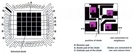
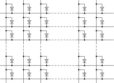
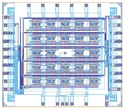
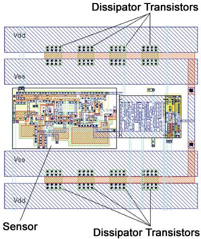
The Infineon thermal test (Figures 1 and 2) die is cell structured. One cell is 0.63 x 0.63 mm, and consists of a heating resistor and a diode sensor. The diodes of the cells are connected in a matrix, assuring scalability of the design. The resistors of the cells in one row are connected in series and the rows may be connected in parallel, assuring large versatility of the test dies.
Figure 1. One cell and the chip layout of the Infineon test die.
Figure 2. Infineon G423 , connection of the diode sensors.Thermal Engineering Associates (TEA)
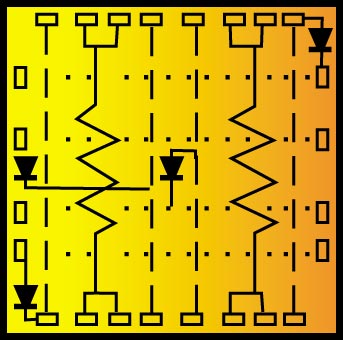
TEA offers a series of thermal test dies. The die family referred to as the TTD-100x series is designed to cover a wide range of applications. The dies are arrayed to produce combinations without having to use internal bond wires. Each die (Figure 3) has four separate diodes, one in the middle, two in opposite corners, and one in the middle of a side edge. Access to all individual diodes is maintained when the dies are array scribed. Each die has two heating resistors that can be operated in series or in parallel to match the capabilities of the thermal test instruments. The dies are sold only in wafer form. [4]
Figure 3. The layout arrangement of TTD-1000 of TEA.NMRC
The NMRC PMOS3 Package Performance Monitoring test chip is presented in [5]. The chip is 5.8 x 5.8 mm and contains 94 pins of 0.1 x 0.1 mm. The chips are fabricated on a wafer measuring 100 mm in diameter and 0.5 mm in thickness. The heaters are two resistors of 300 . The maximum voltage allowed on the resistors is 50 V, and the maximum total power is 16 W. For temperature sensing, the emitter base diode of a lateral pnp transistor is used.IMEC
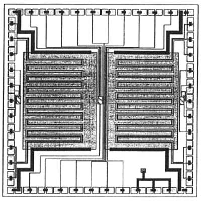
The IMEC test die (Figure 4) consists of 5 x 5 mm cells, which are actually full chip designs. Each has two uniform heater resistors of 25 and three sensor diodes (one in the middle of the chip, two in the middle of side edges). The maximum dissipation is about 15 W. [6]
Figure 4. Layout arrangement of the IMEC PTCA thermal test chip. The diodes are the 3 small hatched rectangles along the horizontal symmetry axis.TUB-TIMA
The THBII thermal benchmark chip (Figure 5) [7] was the first to offer heating and sensing patterns, which are both controllable digitally from an external computer program. It was realized by the 1.2 mm CMOS process of AMS (Austria Mikro Systeme International AG). The test die contains a 2D matrix of identical cells consisting of a dissipator element and a digital output temperature sensor circuit, the THSENS-F sensor [8], and some glue circuitry needed for the addressing of individual dissipator and sensor elements. Size of the cell matrix in the actual chip is 5 x 5 mm as shown in Figure 5. The center cell is a special one containing only the pn diode.
Figure 5. The layout of the THBII thermal test chip of TUB-TIMA.The detailed layout of the dissipator/sensor cell appears in Figure 6. The dissipator element is a MOS transistor, which is split into eight segments that placed regularly on the surface to provide a nearly uniform heat distribution on the cell. The gate voltage of the dissipator transistor is switched in a binary manner. A D-flop is inserted into the cell in order to store the actual on/off state of the dissipator. The dissipation of a single cell is about 50 mW. This means that the maximum dissipated power is 1.2 W.
Figure 6. Layout of a dissipator/sensor cell of the THBIIchip.The main advantage of this chip is the high versatility that enables interesting experiments involving the chip-inside thermal coupling effects in various packages [7]. The problem of the chip is the relatively low dissipation value and the fact that it is not JEDEC compliant. Both of these problems are overcome in the recently designed test die of MicReD and TIMA.
Figure 7. Layout arrangement of the MicReD-TIMA chip.MicReD-TIMA
This multi-functional thermal test die (Figure 7) was designed and created in the framework of the PROFIT project. Its aim was to fulfill the following requirements:
- Support thermal transient measurements with multi-channel test equipment [8] to obtain both single (driving) point and multi-port (transfer) thermal impedances via entirely computer controlled measurements.
- Enable static surface temperature distribution measurement, such as for multiport heat transfer characterization.
- Enable thermal transient measurements and static temperature distribution measurements via the boundary scan (BS) [9] as a demonstrator for the “tester on the die” principle, enabling testing even without test equipment [10]. Boundary scan is the IEEE standard circuitry facilitating the electrical testability of integrated circuits and boards.
- Be modular.
- Be available in the form of bare dies in small sizes, and in the form of IP (Intellectual Property) designs for large sizes.
The dissipation patterns are programable by external asynchronous signals set by the control software. High dissipation levels are provided with homogeneous distribution. The high precision sensor elements provide both analog and/or digital outputs. The BS interfacing assures that thermal measurements with the test chip can be accomplished with the help of a computer program even without an external test system. Production by means of the standard, mainstream CMOS process ensures high quality chips.
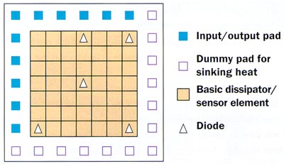
The chip area is mostly covered by an array of cells, each containing a heater resistor and a temperature sensor, which is the latest version of the current output CMOS temperature sensor of MicReD (THSENS-I), [8]. The sensor elements are switched to a single current-frequency converter oscillator circuit through an analog multiplexer. This way a selected current output sensor and the oscillator provide the functionality of the THSENS-F frequency output sensor.
These sensors can be addressed via the BS path, and the measured temperature values are also read out through the BS path. The input and output pads enable both direct and BS measurements. These pads are placed along two edges of the chip while the dummy pads along the opposite edges serve only to emulate heat removal through the bonding wires. Further sensing elements (diodes) are at the chip center, in three corners and at the middle of one edge. The diodes are accessible directly from the pads. For producing larger size test arrays, the test chips are to be manufactured in groups of four as shown in Figure 8.
Figure 8. Suggested fabrication of the chips.
Representative Comparison of Some Available Thermal Test Dies
Most of the test dies found by the author comply with the dissipator and sensor prescriptions of JEDEC, but some do not comply with the requirement for the 85% heater coverage. Detailed comparisons of the thermal test dies for which information could be obtained appear in Table 1.
The software controllability of the dissipation and sensing pattern is an important new feature of the recently designed thermal test dies. This feature can be well exploited if measured with computer controlled multi-channel thermal testers.
Thermal test dies are usually needed in small quantities. The major problem in producing thermal test dies lies in the fact that sophisticated thermal test dies need well established expensive fabrication technologies. Consequently the price of a large test die fabricated with an expensive technology can be prohibitively expensive if it is fabricated in small quantities.
A new approach, the thermal test die in the form of an IP, may help solve this problem. In this case, only the design is sold in the form of a file containing the design description in some kind of standard hardware or IC design description language. This means the thermal test dies can be bought in the form of design files, and chip manufacturers, who are the primary users of test dies, can fabricate these expertly designed test dies for themselves, assuring the best match of silicon thickness.
Conclusions
Thermal test dies are gaining importance with the increasing power densities in packages. Although most of them were designed for DC measurements, they can be used for thermal transient qualification as well. Multi-channel transient testers deliver temperature data from different parts of the package simultaneously, which can be very advantageous if, for example, the efficiency of various cooling conditions is the subject of experimentation.
With the new measurement tools and methods, test dies are getting more sophisticated as well. Such test dies are expensive to fabricate, hence it is cost effective for most users to buy them ready made. However, it is not easy to find information about the available thermal test dies. To bridge this gap the author has tried to collect all the public information about test dies. Moreover, the author will continue to update the information in this article as new information regarding other available thermal test dies becomes available from the various vendors.
Acknowledgments
The author wishes to acknowledge the help of B. Courtois, C. Villa, J. Janssen, H. Pape, B. Siegal, A. Claassen, Zs. Benedek, A. Poppe, G. Kelly, V. Sz�kely and L. Pohl in collecting the data and/or commenting on this paper.
References
1. EIA/JEDEC Standard EIA/JESD51-4 � “Thermal Test Chip Guideline (Wire Bond Type Chip)”, February, 1997.
2. Alan Claassen, H Shaukatullah: “Comparison of Diodes and Resistors for Measuring Chip Temperature During Thermal Characterization of Electronic Packages Using Thermal Test Chips”, Thirteenth IEEE SEMI-THERM Symposium, 1997.
3. D.L. Rodkey: Manual for Using Delco Electronics’ Thermally Sensitive Die”, Delco Electronics, Jan. 30, 1987.
4. www.thermengr.com
5. National Microelectronics Research Centre: “PMOS3 Package Performance Monitoring Test Chip”, Cork, Ireland.
6. Filip Christiaens: “Thermal Modeling and Characterization of Electronic Components: Steady-State and Transient Analysis”, Katholike Universiteit Leuven, In samenwerking met IMEC vzw Januari 1998.
7. Sz�kely V., M�rta Cs., Rencz M., V�gh G., Benedek Zs, T�r�k S.: “A Thermal Benchmark Chip: Design and Application”, IEEE Transactions on Components, Packaging, and Manufacturing Technology � Part A. Vol. 21. No. 3, Sept., 1998.
8. www.micred.com
9. H. Bleeker, P. van den Eijnden, F. de Jong: “Boundary Scan Test: A Practical Approach”, Kluwer Academic Publishers, Dordrecht, 1993.
10. V. Sz�kely, M. Rencz, A. Poppe, B. Courtois : “New Way for Thermal Transient Testing”, Proc.of SEMITHERM, pp182-189, San Diego, CA, USA, 1999.

