Thermal experts generally view thermal resistance as a measurable property of a semiconductor device. A system designer, who designs an appliance, is usually not a thermal expert. The system designer just needs a way to determine the size of the external heat sink. At high heat sink temperatures, less power dissipation is allowed in the device. The ratio at which case temperature can be exchanged with dissipated power has the unit of thermal resistance (K/W), but is not related to a real temperature occurring anywhere in the device. This paper describes how this virtual junction temperature can be used to specify the thermal properties for a power IC.
 |
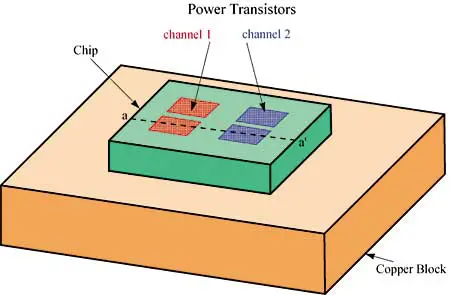
Figure 1. Power device with two channels.
Section 1 describes a typical power IC, taking an audio power amplifier as an example. Because we must deal with multiple heat sources and large temperature differences within the same chip, it is necessary to employ a thermal resistance network instead of the commonly used thermal resistance value. In Section 2, the concept of virtual junction temperature is introduced, leading to the definition of thermal resistance in relation to the rating system. The rating system (defined by the IEC standards) describes the division of responsibility between the component manufacturer and the system designer. Section 3 outlines a way to determine the thermal resistance network.
Section 1: Characteristics of a Power IC
Power devices consist of a die that is attached (usually with solder) to a copper block. This copper block is visible at the bottom of the package and should be mounted on a heat sink (Figure 1). This is the dominant path for the heat flux. Contrary to the packages targeted by the DELPHI/SEED projects [1,2], the heat fluxes through the top, sides and leads can be neglected without introducing significant errors. This does not mean that a single thermal resistance is sufficient to characterize a power device. A thermal resistance network is still needed to model the different modes of power dissipation due to the multiple heat sources.
Most power ICs contain several sources of heat on the die that can dissipate independently. An example of such a device is a stereo amplifier. If, with such a device, only one of the two amplifiers is used in an application, and the other does not dissipate any power, the total dissipation will be constrained to a smaller part of the total chip area. Locally, the heat flux density increases, so with the same total dissipation, higher temperatures will result. Hence, a larger thermal resistance value must be used for the heat sink calculation.
The two power stages are placed side by side on the die. Heat flow is mainly from top to bottom, but some heat also flows in a lateral direction. Both output stages can also be used independently. The curves in Figure 2 show the temperature profile across the die for three cases: both channels dissipating and each channel individually.
With both channels dissipating, the power dissipation is twice as high, but the temperature is not. Similar to DELPHI/SEED, a thermal resistance network can be constructed that gives accurate results for all three cases. These resistances characterize the allowed combinations of power dissipations and case temperatures and have, strictly speaking, no physical meaning.
The thermal resistance value is only valid for one main application, in this case where all power transistors have the same dissipation. To facilitate virtual junction temperature calculations for different applications, a thermal resistance network may be specified in addition to the single thermal resistance value. This thermal resistance network gives a simplified representation of the individual thermal resistances together with the mutual thermal coupling. For the main application, a single thermal resistance value can still be given that may serve as a figure of merit.
 |
Figure 2. Temperature profile across a – a’ with channel 1, channel 2, and both channels dissipating.
Section 2: Thermal Ratings and Virtual Junction Temperature
The removal of the dissipated heat inside a power semiconductor device is the joint responsibility of the device manufacturer and the equipment designer. The temperatures that occur at the top of the die must be limited. At lower case temperature, a higher level of dissipation can be allowed. The thermal limits of a semiconductor device are specified by appropriate ratings.
The objective of a rating is to define the division of responsibility between the manufacturer of a semiconductor device and the equipment designer. A rating is a limiting value of operating conditions, which may not be exceeded. This limiting value is chosen by the device manufacturer to provide acceptable serviceability of the device [4].
In the past, the relationship between allowable power dissipation and case temperature was defined by a power derating curve. The thermal limits of a semiconductor device can also be specified by two ratings: the maximum virtual junction temperature and the maximum power dissipation.The IEC 747-1 definitions of the virtual junction temperature Tvj, the case temperature Tcase and the thermal resistance from junction-to-case Rth vj-case will be used throughout this text [3]. The following expression holds:
Tvj = Tcase + PD . Rth vj-case
This expression may be regarded as an alternative definition of Tvj. Hence, the virtual junction temperature is not a real temperature occurring anywhere inside the device. It is a quantity that is calculated from the case temperature, the dissipated power and the value of the thermal resistance supplied by the device manufacturer. This idea of a thermal resistance as a value that is chosen by the device manufacturer may be counter intuitive to experts on thermal matters, since they usually consider the thermal resistance as a measurable characteristic of the device.
The device manufacturer specifies a maximum rating for the virtual junction temperature. This maximum value is determined by the design rules of the process technology and is usually 150oC for audio power amplifiers. This is very similar, for example, to the rating of the maximum supply voltage. The design rules for the process technology are verified with life testing of the products and with life testing of relevant special test structures.
The maximum rating for the virtual junction temperature forces the equipment designer, when considering all possible combinations of case temperature and power dissipation, to take care not to exceed the maximum value of the virtual junction temperature. The equipment designer can verify compliance to this by measuring the case temperature and the power dissipation. The case temperature can be measured using a thermocouple; the power dissipation can be measured by measuring voltages and current. To the equipment designer, the thermal resistance has a fixed value and is not subject to any spread.
Section 3: How the Thermal Resistance Network Is Obtained
During the design of a power IC, thermal considerations play a very important role. Once the approximate size of the power transistors and their location relative to each other is known, the temperature distribution in the application can be calculated using a three-dimensional finite difference model. Such a model can become quite large, but, because heat is exclusively removed by conduction, the basic equations are simple.
For a representative number of different applications the power, as expected, is used as a boundary condition for the simulation. The bottom of the copper block, which normally connects to the heat sink, is kept at zero temperature (infinite heat sink). The interface resistance between power device and heatsink is not taken into account.
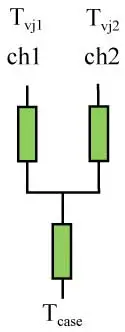
From the resulting temperature profile at the top surface of the die, the average temperatures of all relevant power transistors are calculated. A resistor network that provides a best fit to all boundary conditions can now be constructed. Preferably, the network should be a tree since this allows easy hand calculation of the virtual junction temperatures without the need for a circuit simulator. (See Figure 3.) The temperature dependence of the conductivity of silicon must be included. The main source of variability of the actual temperatures in a device is the die attach quality. The die attach quality is usually 100% tested on all products using a thermal transient test [5].
 |
Figure 3. Thermal resistance network.
Of course, the reject limits of this test must be taken into account in determining the thermal resistance network. The thermal resistance network mainly depends on the chip area and location of the power transistors inside the power IC, and, to a lesser extent, on the package and die attach properties.
Conclusions
A single thermal resistance value is not sufficient to specify a power IC. A thermal resistance network is needed. In this thermal resistance network, the resistances have fixed values. The virtual junction temperature calculated with such a model is no physical temperature, but represents the allowed combinations of case temperature and power dissipation in various parts of the circuit.
Contrary to the real temperatures inside a product, the virtual junction temperature can be measured, or, more precisely, calculated from the measured power dissipation and the case temperature. The power dissipation of various circuit parts can be calculated from all pin currents and voltages. The case temperature can be measured with a thermocouple. This helps to clarify the division of responsibility between the IC manufacturer and the system designer who uses the IC. The single thermal resistance metric for the nominal application can still serve as a figure to compare different products.
Strictly speaking, by specifying a rating for the virtual junction temperature rather than the ‘real’ junction temperature, the equipment designer may design his application so that the ‘real’ junction temperature may have any value no matter how high. The designer must only limit the combination of case temperature and power dissipation so that the calculated virtual junction temperature remains below its rating at any time. Hence, it is not the ‘real’ temperature that is limited, but rather the stress conditions that lead to the ‘real’ high temperatures.
References
1. H. Rosten , C. Lasance, J. Parry, “The World of Thermal Characterization According to DELPHI-Part I: Background to DELPHI”, IEEE Trans CHMT vol.20, 1997, pp. 384-391.
2. C. Lasance, H. Rosten , J. Parry, “The World of Thermal Characterization According to DELPHI-Part II: Experimental and NumericalMethods”, IEEE Trans CHMT vol.20, 1997, pp. 392-398.
3. IEC 747-1 “Semiconductor Devices”.
4. IEC 134 “Rating Systems”.
5. SEMI G46 “Thermal Transient Testing for Die Attachment Evaluation”.


