This column has emphasized methods of analyzing packages in the JEDEC-standard test environment. A thermal metric that lends itself to analyses of system applications is the junction-to-board thermal characterization parameter, JB. If one knows the board temperature (TB), then the junction temperature (TJ) can be determined by a simple application of the following formula:
TJ = TB + P � JB(1)
where P is the power applied to the device.
It is difficult to calculate the temperature distribution over the surface of populated printed circuit board (PCB) using analytical methods, due to its complicated geometry. However, here we use a simplifying assumption to make the calculation more accessible. The basis of the technique is to convert the multi-package situation into a single-package model involving the package of interest.
The method is as follows: calculate the area of the single-package board from the following formula:
 |
where An and Pn are the footprint area and applied power for package n, ATotal is the area of the entire PCB, and PTotal is the total power applied to all packages. One then constructs a single-package model with a square board having the indicated area and with the appropriate heat load, Pn, applied over the package footprint area and solves for the board temperature within the package footprint.
 |
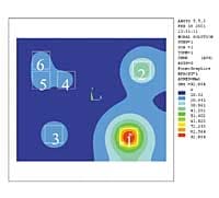
Figure 1. Result of an analysis of a PCB containing six packages.
We evaluate the accuracy of this simple model by performing a thermal analysis using the Finite Element Method applied to a situation typical of a PC motherboard and then performing a series of single-package analyses and comparing the results. Figure 1 displays the result of an analysis of a PCB containing six packages. The indicated temperatures are relative to the air temperature. The package sites are numbered 1 through 6. Each is 35 mm sq. The power levels are 10, 4, 2, 1, 1, and 1 W, respectively. The board has the following characteristics: 300 x 250 x 1.6 mm, kx-y = 14 W/mK, kz = 2 W/mK, h = 10 W/m2K (applied to each side of board).The dimensions and thermal conductivity values are typical of a PC motherboard. The largest value of board temperature minus the air temperature is 92.8oC at the location of the 10 W load.
 |
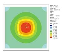
Figure 2. Thermal solution for a single-package model with a 100 mm sq. PCB.
Figure 2 illustrates the thermal solution for a single-package model with a 100 mm sq. PCB having the same thickness, material properties, and boundary conditions as that in Figure 1. A heat load of 1 W is applied over a 35 mm sq. area. In this solution, the peak temperature rise is 10.3oC per Watt of applied power. In the single board model, this quantity is defined as BA.
 |
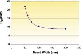
Figure 3. Relationship between BA and the width of the board.
Figure 3 shows the relationship between BA and the width of the board, calculated in the manner of Figure 2 at a range of values of board width between 50 and 200 mm.
|
Table 1. Summary of Values of (TPeak,n – TAir)/Pn for Each Package Location on the PCB
Table 1 summarizes the values of (TPeak,n – TAir)/Pn for each of the package locations on the PCB. It also provides the value of the width of the board calculated using Equation 1, the subsequent value of BA, and the percentage difference between
BA and (TPeak,n – TAir)/Pn
The percentage error varies from 0.5% to 20%. As might be expected, the error will be greater for packages close to some other package or to the edge of a board. However, this level of accuracy is surprisingly good for such a simple calculation. The single-package equivalent model can, therefore, be useful in providing a rapid estimate of board temperature with a moderate level of accuracy.
[In this context, the reader may find useful an analytical method for calculating BA for a single-package model. Such a method was described in this column in the September 1998 issue.]


