Introduction: The Need for IC Surface Measurement Techniques
Current trends in microelectronic design generate challenges in both the design and test of integrated circuits (ICs). One area that has been gaining increased relevance with regard to the microelectronic evolution is thermal management/analysis, which proves essential in the domain of IC design to prevent reliability problems or circuit performance degradation due to the increase of power dissipation levels reaching tens or even hundreds of Watts [1].
Temperature plays an important role in the field of IC test and verification. For instance, temperature measurements of the silicon surface can be used to detect the structural integrity of the circuit under test or that of the solder layers in the package. Examples of this technique, known as thermal testing, can be found in [2,3].
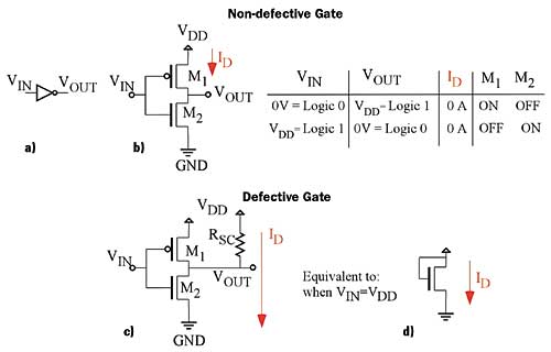 |
Figure 1. Schematic of a fault-tree and faulty CMOS logic inverter. The conducting state of the transistors is indicated in the table for the different values of the VIN voltage.Let us focus on the detection of structural defects in a circuit. If a circuit has a structural defect, some of its devices may dissipate power levels different from the nominal ones, and these different power levels may, in turn, alter the surface thermal map of the silicon surface. Figure 1 shows a typical example of what may happen in a digital circuit: a short circuit appears between the supply line, VDD, and the output line of an inverter. The electrical model of this kind of short circuit is a resistor, RSC, that usually has a low value. Therefore, when a logic one drives this gate, current flows from VDD to GND, the NMOS transistor, M2, behaves as a heat source, and a hot spot appears. Thermal measurements of the IC surface can detect this kind of defect.
Depending on where these measurements are taken and on the information that the test engineer seeks to extract, several techniques may be employed to perform these measurements. For instance, after manufacturing an IC, it would be interesting not only to detect a defective circuit but also to locate and to characterize it. This would be a good way to provide feedback information to design and process manufacturing engineers and could help avoid the placement of potentially defective structures in future designs or could enhance the fabrication process. The performance of instrumentation for such thermal characterization would require lateral resolution in the micron range and temperature sensitivities in the mK range to provide good spatial and thermal characterization.
Currently, there is a worldwide research activity in the field of temperature measurement techniques and temperature sensor design for test applications. In this article, among the different techniques currently available, we will discuss two advanced laboratory measurement techniques: the scanning thermal microscope method and the laser thermoreflectometer method. We will present measurements performed on an IC sample designed to characterize thermal couplings generated by defective gates. Specifically, the IC contains several structures like the one plotted in Figure 1d and some built-in temperature sensors. This sample has allowed us to compare the performances of different surface temperature measuring techniques.
Detection of Hot Spots with a Scanning Thermal Microscope
The scanning thermal microscope (SThM- Topometrix®) is a conventional atomic force microscope (AFM) mounted with a specific probe. The AFM system allows us to control the tip position and contact force with the sample. Monitoring is performed with a feedback loop between the signals of three x-y-z piezo-electrical ceramics carrying the tip cantilever and of four photodiodes tracking a laser beam which reflects on the probe.
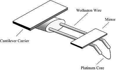 |
Figure 2. Schematic of the SThM thermal probe.The probe is a Wollaston wire shaped as a tip and etched to uncover the core platinum(Pt) wire (Figure 2). The Pt wire is used as a thermal resistor. At constant input current, the tip voltage is measured while scanning the surface so that the Pt wire electrical resistance can be calculated at each point on the sample surface. The AFM is used in contacting mode so that thermal equilibrium is achieved between the probe and the surface. A preliminary calibration allows us to relate temperature variations to electrical resistance variations to an accuracy within 10%. The contact radius of the tip can be estimated to 50nm [4], its diameter being 5 microns. A laser beam reflects on the mirror to detect z-deflections of the cantilever with nanometer precision, allowing us to extract topographic maps of the IC surface.
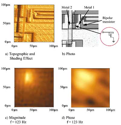 |
Figure 3. Topographic and AC temperature measurements performed with the SThM.Figure 3 shows measurements performed with the SThM. Figure 3a shows a processed topographic image while 3b shows a photograph of the same location on the layout. Comparing Figures 3a and 3b allows us to easily identify and locate the metal lines and devices (i.e., the MOS transistors acting as heat sources and a bipolar transistor). If the power dissipated by the heat source is a harmonic function, i.e., P(t)=PMAX�cos(wt), then the temperature at a distance, r, from it would be T(t,r)=TMAX(r)�cos(wt+(r)). The measurement of both amplitude, TMAX(r), and phase,
(r), can be achieved by processing the information provided by the sensor with a lock-in amplifier. These so-called AC measurements have been shown to be more sensitive when used to detect hot spots in ICs. Also, they are more useful for characterizing thermal coupling between devices because coupling thermal transfer functions can be derived from them.Figures 3c and 3d show AC (magnitude and phase, respectively) temperature measurements obtained when the heat source is modulated at a frequency of 123 Hz. Although the oxide and passivation layers placed over the silicon attenuate the temperature signal, the system sensitivity is sufficient to detect and locate the hot spot. Higher sensitivity is observed in phase measurements than in amplitude measurements. Note that the metal line, which acts as a heat spreader, attenuates both the phase and amplitude signals. The time needed to extract the images in Figure 3 is about two minutes.
Detection of Hot Spots with a Laser Thermoreflectometer
A thermoreflectometer exploits the proportionality betwee n the variation of a material’s reflection coefficient and the surface temperature changes of that material. If a laser beam is focused on a silicon surface and the reflected light is sensed with a photodiode, variations of the current, I , generated by changes of the reflection coefficient can be related to the variations of the temperature, T, of the area to which the laser points [5]:
 |
The exact value of the constant depends on the material and the light wavelength, and can be found in the relevant literature. However, when the laser beam reaches the silicon surface through silicon dioxide and passivation layers, this coefficient is affected by a scaling factor that can be greater or smaller than unity, depending on the thickness of these layers [6]. Results reported in [7] show the laser probe to be a fast surface thermometer (up to 150 MHz) with an excellent lateral resolution (1 �m) and large dynamics (
T from 10-3 to 102 K).
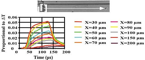 |
Figure 4. Example of amplitude transient temperature measurements performed with the laser thermoreflectometer.Figure 4 shows an example of transient measurements. At the top of the image is a photo of the activated heat source and an axis where different measurements have been performed. Following this line, the thicknesses of oxide and passivation layers are assumed to be homogeneous and, therefore, so is the constant, . The heat source has been activated with a power pulse of 23 mW for a duration of 100 �s. Temperature waveforms have been extracted at different distances from the heat source. In this example the diameter of the laser beam is 3 mm, therefore measurements can be assumed to be highly localized. As can be seen, the bandwidth of the measurement probe allows us to monitor the temperature waveforms that occur at the silicon surface. The system allows us to perform AC measurements as well. Therefore, accurate transfer functions of thermal coupling between two points can be extracted.
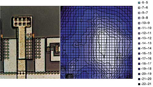 |
Figure 5. Bidimensional phase AC thermal map produced with the laser thermoreflectometer.By repeating these highly localized measurements over an area of the IC, surface thermal maps can be obtained. As an example, Figure 5 shows the phase map (60 x 60�m) obtained for AC measurements. Comparing the phase map with the layout of the scanned area, the activated heat source is easily located. The advantage of phase measurements in front of amplitude measurements is that they are not affected by changes in the coefficient, , generated either by changes in the material at which the laser is focused or by changes in the thickness of the passivation and oxide layers placed over the silicon. The time needed to extract the images of Figure 5 is about one hour.
Discussion
Traditionally, thermal maps in integrated circuits have been extracted in a laboratory environment by using either infrared thermography [8] or contrast materials, such as liquid crystals [9] or phosphors [10].
We have presented two alternative techniques, which offer high spatial and thermal resolution with interesting dynamic capabilities, and which can be used for different applications in addition to the detection of heat sources in ICs [13,14]. Other techniques offer similar performance, such as laser interferometry [6], which measures surface displacements and surface displacement gradients due to thermal expansions. This technique is powerful in the sense that it gives access to surface stress levels due to thermal expansions and predictions of IC failures, in addition to thermal characterization. Built-in temperature sensors have also been used to characterize thermal couplings in ICs as well as to detect faulty ICs. Reference studies can be found in [11] and [12]. The advantage of these systems is that they directly measure silicon die temperature without being affected by layers placed over the silicon. They can also be used in both laboratory and industrial environments.
Summary
We have emphasized the need for surface temperature measurements for IC design and test applications. Focusing on test, we have shown how heat sources appear in defective ICs due to short circuits between two metal lines.
We have discussed the principle of the scanning thermal microscope technique and presented representative measurements. The scanning thermal microscope probe has simultaneous topographic and temperature sensing capabilities, and therefore allows an easy identification of the active heat source. However, the measurements are affected by the attenuation of the layers placed over the heat source, such as metal lines and silicon dioxide and passivation protection layers. The laser thermoreflectometer offers highly localized measuring capabilities, high bandwidth and sensitivity. It allows the extraction of the thermal coupling transfer function between a heat source and a point of the silicon surface. Finally, we have mentioned other surface temperature sensing strategies, and delineated several points for comparison.
Acknowledgements
The authors wish to thank Dr. Bruce Guenin and Prof. Antonio Rubio for their assistance in developing this article, and Mr. Jean Michel Rampnoux for his work in the experimental set up.
References
- International Technology Roadmap for Semiconductors, Semitech, http://public.itrs.net/
- Altet, J., Rubio, A., “Built-In Dynamic Thermal Testing Technique for ICs”, Electronic Letters, Vol. 32, No. 21, October 1996, pp. 1982-1984.
- Sz�kely, V., Rencz, M., Poppe, A., Courtois, B., “New Way for Thermal Transient Testing,” 15th IEEE SEMITHERM Symposium, March 1999, pp. 182-188.
- Majumdar, A., Review of Scientific Instruments, 1998
- Claeys, W., Dilhaire, S., Quintard, V., Dom, J.P., Danto, Y., “Thermoreflectance Optical Test Probe for the Measurement of Current-Induced Temperature Changes in Microelectronic Components,” Quality and Reliability Engineering International, Vol. 9, 1993, pp. 303-308.
- Quintard, V., Deboy, G., Dilhaire, S., Lewis, D., Phan, T., Claeys, W., “Laser Beam Thermography of Circuits in the Particular Case of Passivated Semiconductors,” Microelectronic Engineering 31, Elesevier, 1996, pp. 291-298.
- Claeys, W., Dilhaire, S., Jorez, S., Pati�o-L�pez, L.D., “Laser Probes for the Thermal and Thermomechanical Characterization of Microelectronic Devices,” Microelectronic Journal, 32, Elsevier, 2001, pp. 891-898.
- Lee, D.H., “Thermal Analysis of Integrated-Circuit Chips Using Thermographic Imaging Techniques”, IEEE Transactions on Instrumentation and Measurement, Vol. 43, No. 6, December 1994, pp. 824-829
- Nishiguchi, M., Fujihara, M., Miki, A., Nishizawa, H., “Precision Comparison of Surface Temperature Measurement Techniques for GaAs IC’s,” IEEE Transactions on Components, Hybrids, and Manufacturing Technology, Vol. 16, No. 5, August 1993, pp. 543-549.
- Kolodner, P., Tyson, J. A., “Remote Thermal Imaging with 0.7-mm Spatial Resolution Using Temperature-Dependent Fluorescent Thin Films,” Applied Physics Letters, Vol. 42, No. 1., January 1983, pp. 117-119.
- Altet, J., Rubio, A., Dilhaire, S., Schaub, E., Claeys, W., “Thermal Coupling in Integrated Circuits: Application of Thermal Testing”, IEEE Journal of Solid State Circuits, Vol. 36, No. 1, January 2001, pp. 81-91.
- Sz�kely, V., M�rta, Cs., Koh�ri, Zs., Rencz, M., “CMOS Sensors for On-Line Thermal Monitoring of VLSI Circuits,” IEEE Transactions on Very Large Scale Integration Systems, Vol. 5, No. 3, September 1997, pp. 270-276.
- Dilhaire, S., Jorez, S., Pati�o-Lopez, L.D., Claeys, W., Schaub, E., “Laser Diode Light Efficiency Determination by Thermoreflectance Microscopy” Microelectronics Journal, Vol. 32, 2001, pp 899-901.
- Dilhaire, S., Jorez, S., Patino-Lopez, L.D., Batsale, J.C., Claeys, W., “Thermoreflectance Microscopy: Calibration of Temperature Measurements upon Micrometric Metal Lines Applied to Thermal Conductivity Identification of Micrometric Dielectric Layers”, Heat Tansfer and Transport Phenomena in Microsystems, Proceedings, October 15-20, 2000, pp. 392-397, 2000.


