By now, it is a tired truism to say that the consumer electronics industry has consistently delivered on its promise to provide products that are smaller, faster, and more feature-rich at an ever cheaper price. The main driver for these trends has been the increasing integration of more functions on a single chip. In spite of its greater performance, the PC of today has far fewer chips, packages, boards, and subassemblies than the PC of 10 years ago. Furthermore, the computational power in the hand-held devices of today, such as a personal data assistant (PDA), would be impossible without the high level of on-chip integration now available.
The trend towards greater integration of functions into a single chip has simplified the system hardware, but has also led to greater complexity at the package level. This is due to the fact that each chip has a greater number of input/output channels (I/O’s).
The need for managing more I/O’s in a smaller space drove packaging technology to the development and widespread use of what are commonly called Ball Grid Array (BGA) packages.
Ball Grid Array Package Construction
BGA packages contain a laminated substrate or printed circuit board (PCB), produced by a refined version of the same technology used to produce motherboards. The conductors consist of traces etched in copper foil bonded to a polymer substrate. PCB technology permits BGA packages to have several layers of conductors and planes with the inter-layer connection provided by through-hole plated vias. The electrical connections to the chip are eventually routed to an array of solder balls attached to the bottom of the substrate, which function as leads. Figure 1 illustrates the internal design of a classic plastic BGA (PBGA) package.
 |
Figure 1. Cross-sectional view of PBGA package soldered to a PCB.
Differentiating Features of PBGA Packages
Once the first PBGA packages were commercialized it was inevitable that new designs would proliferate. Most of the internal features of the PBGA package are determined by the patterns in the CAD drawings, which are replicated in the photolithographic process used in PCB manufacture. A few strokes of the designer’s mouse can dramatically change the internal construction of the package.
 |
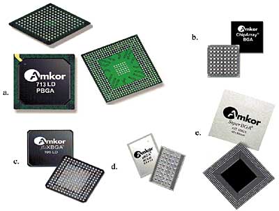
Figure 2. Various BGA packages: a. PBGA package, b. near-chip-scale package with BT substrate, c. BGA package with tape substrate; balls attached to top metal through perforations in tape, d. chip-scale BGA with tape substrate and compliant die attach, e. thermally-enhancd BGA package with heat spreader bonded to substrate. [2]This article attempts to categorize the many ways in which one BGA package can differ from another by focusing on external and internal package features individually. Figure 2 depicts a number of BGA package formats, which embody many of the features described below.
External Features
Body Size
BGA packages can range in size from chip-scale packages of a few millimeters on a side to very high leadcount packages upwards of 50 mm. The body size is determined primarily by the need to fit a certain number of leads at a pre-determined pitch.
Ball Pitch
The ball pitch is determined by the need to pack more leads in a given amount of space. The largest pitch commonly in use is 1.5 mm. The smallest, at the present time, is 0.5 mm. There is a cost increase associated with migrating to a smaller pitch, due to the requirements for more precise drilling and etching technology.
Ball Matrix
Typically the balls are on a rectangular grid. The ball matrix indicates the number of balls along two adjacent outer rows from corner to corner. For example, a package with a 26 x 26 ball matrix would have 26 balls on each outer row, a so-called “square” matrix. A package with differing numbers of balls on adjacent outer rows is said to have a “rectangular” matrix.
A package in which all possible sites within the matrix are occupied by solder balls has a “full” matrix. Packages for which this is not the case have a “depopulated” region. This can be the entire center region, so that the package has only “peripheral” rows, or it can have peripheral rows and a center matrix, with a depopulated region between them.
Mold Cap
Most BGA packages have an overmolded cap to encapsulate the die and bond wires, protecting them from damage in handling. The mold cap also serves to stiffen the assembly. This is important when the laminate is thin and lacks rigidity. Too much bow in the laminate can prevent all of the solder balls under a package from forming a secure joint to the motherboard during the soldering process.
The mold cap can either extend to the edge of the laminate or leave a border between its outer edge and that of the laminate. The mold cap is sometimes eliminated when a flip-chip die is used on a stiff multilayer substrate.
Internal Features
Substrate Material
The most common substrate material is the fiber-reinforced material, BT (bismaleimide triazine). It has enough stiffness that it does not have to be completely covered by the mold cap. It lends itself for use in multilayer stackups, allowing several metal layers to be used if desired. Alternatively, polyimide tape is used in many applications. Due to its flexibility, it must be completely covered by the mold cap. Normally, only one layer of tape is used. The appeal of using tape is that the etching technology is more advanced than that for BT substrates, leading to finer lines and spaces.
Die Attach Material
The choice of material used to attach the die to the substrate and its thickness play an important role in the package thermal performance. In most BGA packages with BT substrates, it is typical to use a silver-filled epoxy for this function. Unfortunately, these materials usually have poor adhesion to the top-layer of metal under the die because of gold plating applied to this metal. It is common practice to leave the solder mask layer intact under the die to promote better adhesion. Due to its very low thermal conductivity, it is desirable to keep the solder mask thickness to a minimum. On occasion, in the interest of enhancing the thermal performance, openings in the solder mask under the die are created to provide localized regions of direct contact between the die attach material and the top metal layer.
In packages using a tape for a substrate material, it is typical to use a thick, compliant die attach layer. This is intended to reduce the stress on the solder balls under the die, resulting from the very different coefficients of thermal expansion for the die and the motherboard and from the fact that the thin tape does not relieve the stress between these two components. The much thicker BT substrates provide adequate compliancy without any added “cushion.”
Substrate Metal Features
Number of Metal Layers – When BT substrate materials are used, there is usually an even number of metal layers. The top and bottom layers are usually used primarily for distribution of the signals. When four layers are used, typically the inner layers consist of a ground and a power plane. When more than four layers are used, the additional layers are typically signal distribution layers. The presence of planes in the substrate can play an important thermal role in spreading the heat to all of the solder balls for transfer to the motherboard.
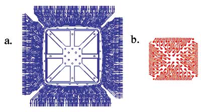
Sub-Die Metal Pattern – In the original PBGA designs, a so-called “die flag” structure was etched in the top metal layer. The die flag was typically routed to the ground plane of the motherboard using a network of vias. The thermal function of the flag is that it captures heat from the die and routes the heat into the via network. It functions as an important part of a thermally enhanced path for heat to flow to the ground plane of the motherboard. Figure 3a illustrates a typical die-flag structure.
 |
Figure 3. Examples of top-metal patterns: a. die flag and fan-out pattern, b. fan-in trace pattern with no die flag.Many chip-scale packages need the full area of the laminate for routing signals to the motherboard. Hence there is insufficient room to place a flag under the die. In these situations the sub-die metal consists of traces routed to vias to carry the signals to the appropriate solder balls, as shown in Figure 3b.
Signal Trace Pattern – In the classic PBGA design, all of the traces are routed in a radial direction away from the die. This is called a “fan-out” pattern. The other extreme is a chip-scale package. In this case, the traces must be routed from the edge of the die toward the center of the substrate. This is referred to as a “fan-in” trace pattern. Figures 3a and 3b illustrate these two patterns.
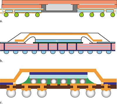
Vias – These are used in packages with BT substrates to route the signals from the top metal layer to the internal and bottom metal layers. They also play an important thermal role in enhancing the through-plane thermal conductivity of the substrate materials. Most of the vias will route signals to solder balls that are connected to traces on the motherboard. The vias that are most effective in transferring the heat to the motherboard are those attached to a die-flag structure and routed to the ground plane of the motherboard. The vias can be either “thru-hole” or “blind.” The thru-hole vias are routed from the top layer of the laminate to the bottom layer (Figure 4a). Clearance regions are etched in a metal layer in the vicinity of a particular thru-hole via when no electrical connection between them is desired. Blind vias are used in high-density substrates (Figure 4b). These vias terminate on the layers they connect. Hence, they do not occupy any “real estate” on the layers beyond those of interest.
 |
Figure 4. Examples of via types: a. thru-hole, b. blind, c. solderIn the commonly used tape designs, the solder from the solder ball itself will function as a via. In these designs, the top-layer metal covers perforations in the tape. The solder contained in the perforation will wet the underside of this metal and conduct the electrical signals to the spherical part of the solder ball (Figure 4c).
First-Level Interconnect
First-level interconnect refers to the technology for providing the electrical connection between the die and the substrate. By far, the most common method uses bond wires. Alternatively, flip-chip technology is used. Wire bond technology provides the advantage that it is possible to use the same substrate with dies of moderately different size. This is accomplished simply by reprogramming the wire bonder to accommodate the different size die. It has been a common method of reducing the cost of a chip by “shrinking” it. In this way, more chips can be produced from the same wafer. When a flip-chip die is shrunk, the substrate must be redesigned.
Single Die/Multi-Die Configuration
Most BGA packages contain only one die. However, it is becoming more common to incorporate more than one die in a package. These multiple dies can be arrayed so that each is directly attached to the substrate. Alternatively, it is possible to use a “stacked die” technology. A die can be attached to another. The top die can be connected electrically to the bottom die using either wire bonding or flip-chip technology. It is possible for the top die to be connected electrically to the substrate using bond wires.
Heat Spreaders
The use of a heat spreader can play a significant role in enhancing the thermal performance of a package. There are three common configurations of heat spreaders:
 |
Figure 5. Example of heat spreader types: a. laminated; b. drop-in;
c. cavity type used with flip-chip
- A planar heat spreader can be laminated to the substrate. The die is attached in a die-down configuration to the underside of the heat spreader through a window cut in the substrate (Figure 5a).
- A heat spreader is formed so it can be “dropped in” to the mold cavity and is embedded in the molding compound (Figure 5b).
- A heat spreader with a cavity is attached in the center to the top surface of a flip-chip die and on the edges to the substrate (Figure 5c).
Presence of Other Electrical Components
 |
Figure 6. Conceptual drawing of System-in-Package design.A package format called a System-in-Package (SiP) has been growing in popularity in recent years. It represents the next step in the evolution of a package from a single device to a complete sub-system. These packages can contain multiple chips and passive components (inductors, capacitors, and resistors). Figure 6 suggests the complexity possible in SiP designs.
Thermal Performance
The thermal performance of a given BGA package is the result of the many features described here. It is beyond the scope of this article to deal with this issue in detail. In general, the most critical features to drive thermal performance are:
- Die size
- Thermal conductivity of die attach material
- The number of vias directly under the die, and the total area of the sub-die metal to which they are attached
- The presence of metal planes in the substrate
- The presence of a heat spreader
When a package has significant heat spreading due to the presence of planes or a heat spreader, the total number of solder balls plays a significant role. Otherwise, it is predominately the number of solder balls routed to the sub-die metal that impact thermal performance.
Conclusions
The development of BGA packages has revolutionized microelectronics packaging. Their fabrication methods have led to an incredible amount of flexibility in customizing a package for any application. Most likely, new package designs will merely represent novel combinations of the features described here. It is hoped that this article will provide the reader with the basis for making sense of future package developments.
References
- Guenin, B. M., “Packaging: Designing for Thermal Performance,” ElectronicsCooling, Vol. 3, No. 2, May 1997, pp 14-19.
- Note: ChipArray, fleXBGA, and SuperBGA are registered trademarks of Amkor Technology, and �BGA is a registered trademark of Tessera Technologies.


