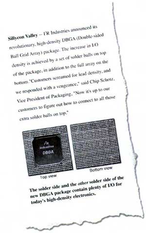
Don’t do a spit-take with your coffee – there is no double-sided BGA. It would never see the light of day, simply because no one would ever buy it. Sure the density is unbeatable, but there is no practical method of soldering all the leads on such a package to a printed circuit board. No electrical hardware design engineer would accept such a ridiculous package. Then why do thermal engineers?
Interconnection technology has been so well worked out over the last 50 years that we now take it for granted. It is hard to believe, but until the 1960s, electronic assemblies were made of discrete components bolted to slabs of phenolic and connected with point-to-point (“rat’s nest”) wiring. Look inside that antique television in your uncle’s basement and you’ll see what I mean.

Getting a comprehensive system of electrical interconnection takes a lot of effort to define all the I/O (Input/Output) paths at every interface. Component vendors think long and hard about electrical I/O before they release a new package.
Why don’t they do the same thing with the Thermal I/O?
Mainly, because hardly anybody thinks that there needs to be a well-defined path for heat to get from the chip to the outside world. Giving it a name should at least get people thinking about it. And giving it an electronic-sounding name like “Thermal I/O” will get much more attention than “heat transfer path.”
Every electrical signal (plus power and ground) has a well-defined, dedicated path to get from the chip to the lead to the solder pad on a printed wire board. The heat generated on that chip needs to have paths from the chip to the outside world that are just as well defined as the electrical I/O.
Heat finds paths out of the chip – whether they are defined out not – through the leads, through the plastic overmold, through air pockets and through decorative labels, if it has to. The problem is, if those paths are not designed in and spelled out, then nobody knows where or how to connect them to a heat sink, or whether a heat sink will do any good at all It’s like getting a 596-ball BGA with no I/O table in the data sheet. You have to guess which signal is on each ball, if any.
Component manufacturers release 30, 50, even 100 Watt parts willy-nilly. Often their data sheets don’t have even a hint that they are aware that an electronic packaging engineer will have to attach some kind of heat transfer gizmo (a heat sink, jet-impingement nozzle, or Freeze Ray courtesy of Batman’s nemesis, Mr. Freeze) to carry those Watts away. Years ago Thermal I/O could be ignored. Power was low, and almost any sneak path for heat was good enough.
But 100 Watt chips are not right around the corner. They are standing on the porch peeking in the front window. So I am invoking my power as a Thermal Guru to decree the following standard. Any vendor not complying with it will be severely made fun of in future columns.
Tony’s Thermal I/O Standard
- Thou shalt clearly define Thermal I/O paths from the chip to the outside of the package. The thermal resistance of each path from the chip to its specified end point on the package surface shall be measured and published.
- Thou shalt talk to customers and find out how they take heat away from boards, then design package Thermal I/O paths that work together with those methods. No more tossing out new package designs and shrugging your shoulders when asked about cooling.
- Thou shalt add to each chip an on-board temperature sensor that can be read externally on dedicated leads while the chip is in operation. That way a customer can tell if a cooling method is actually benefiting the chip inside.
- Thou shalt give the operating temperature limit in terms of the junction temperature, measured by the sensor mandated above, so we have a chance of telling whether your part is getting too hot in our application. No more “70oC ambient” parts.
Perhaps the concept of Thermal I/O will catch on, making our job of cooling electronics a little more possible. I’m just afraid we’ll see the double-sided BGA in production first.


