Wireless communication and advanced radar systems require circuitry that can operate at frequencies greater than 2 GHz and at high power levels. Analog gallium arsenide (GaAs) semiconductors are frequently used in these applications and present additional challenges for thermal engineers compared to silicon semiconductors. Whereas thermal characterization modeling and experimentation for silicon devices typically assumes a uniform distribution of heat generation across the top surface of the semiconductor die, this same assumption is not applicable for GaAs devices.
The thermal conductivity of GaAs is approximately one-third that of silicon, and heat generation is concentrated in a few discrete locations, resulting in large thermal gradients and non-isothermal surfaces. Thermal characterization of GaAs devices requires comprehension of heat generation and temperature prediction within sub-micron length scales. In addition, devices used for power applications have inherently high heat flux densities.
Understanding the thermal characteristics of GaAs devices is important for two primary reasons. The first is that electrical performance of the device is a function of temperature. Electrical parameters of interest that vary with temperature include phase shift, output power, efficiency, and gain. The second reason to understand the thermal performance is to allow prediction of reliability. Thermal modeling is required to accurately correlate temperature-accelerated life test data because of the difficulty in measuring temperatures at such small scales [1]. In fact, it is important that a consistent modeling approach is used to describe the temperatures in accelerated life tests and in applications. The best modeling approach is one that resolves the peak temperature, commonly referred to as the junction temperature.
The cooling of GaAs devices is primarily a conduction problem and requires an understanding of die attach and packaging techniques as well as the device geometry. Convection and radiation are usually present when considering the ultimate heat sink, but conduction is dominant at the device level and is the focus of this article.
Physical Description of Thermal Problem
Understanding thermal issues with GaAs FETs (Field Effect Transistors) and MMICS (Monolithic Microwave Integrated Circuits) first requires some knowledge of the physical characteristics and how the devices operate. A typical GaAs FET consists of several source and drain contacts with gate contacts between them. The contacts consist of metal pads on the surface of the GaAs.
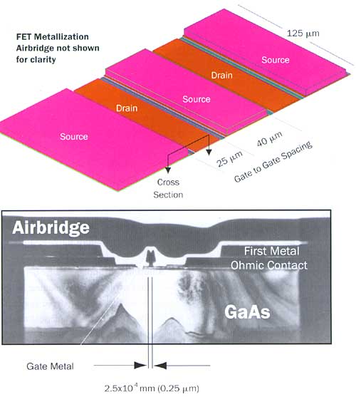 |
Figure 1 GaAs FET metallization and cross section.Figure 1 illustrates the surface metallization for a FET and an electron microscope photograph of a cross section through one gate. The gate metal is the “T” shaped metal with a contact length of 0.25 �m in the photograph. The photograph in Figure 1 also shows the ohmic contact, first metal, and airbridge layers. The airbridge is plated gold that bridges over the gate and drain metal to allow electrical contact between the source pads. Layers designated as ohmic and first metal consist of several vapor deposited metals and may be considered composite layers with non-isotropic thermal conductivity. Continuous gold within the layers accounts for high in-plane thermal conductivity, but layers of titanium and other metals create lower through-plane conductivity.
Gate length refers to the gate-region distance between the source and drain pads (0.25 �m in Figure 1) while the term channel length refers to the length of one channel (125 �m in Figure 1). The sum of the channel lengths is called the FET periphery (a FET with ten 100 �m channels would have a FET periphery of 1000 �m). Figure 1 shows another common parameter in GaAs FET thermal analysis, the gate-to-gate spacing. This spacing may be constant or an alternating pattern. The geometry in Figure 1 was generated from a thermal model of a FET where the gate-to-gate spacing was alternating pattern of 25/40 �m.
Heat Generation and Junction Temperature
The FET junction temperature is often referred to as the finger or channel temperature and is the peak temperature in the GaAs under the gate. Current flow between the source and drain results in resistive heating. The source to drain electrical resistance is dominated by the gate region resulting in most of the heat generation occurring under the depletion region created by the gate. An exact description of where heat is generated is complicated and even becomes dynamic in a pulsed application. However, it is usually sufficient to assume that heat is generated on the top surface of the GaAs under the gate metal or in a volume a few hundred Angstroms thick. The length of the heat-generating region is slightly larger than the gate length and biased toward the drain pad, and a common assumption is that the dimension of the heat-generating region is twice the gate length [2].
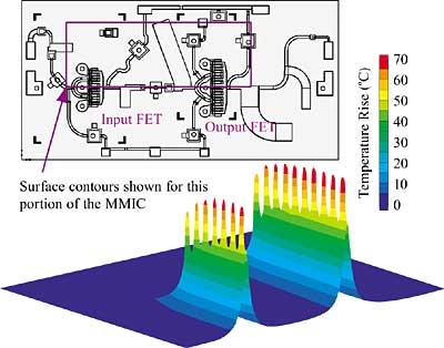 |
Figure 2. GaAs MMIC surface temperature contour plot.Since many applications for GaAs FETs involve amplifiers, the dissipated power is the parameter of interest to the thermal engineer. Dissipated power is the difference between total power input and power output from the device as RF (radio frequency) power. Power added efficiency is a common term that is simply the RF generated power divided by the total input power (electrical and RF). High power amplifiers are currently capable of power added efficiency values in the range of 50 percent. Peak dissipated power levels in GaAs FETs are on the order of 1 W/mm of FET channel length, but actual application values may be significantly less. This limit primarily comes from the breakdown voltage of the GaAs semiconductor, which is slightly less than 20 Volts. It should be noted that efficiency values are often measured at the MMIC level and some of the dissipated power will occur in the RF matching circuitry on the MMIC in addition to the portion dissipated in the FETs.
A top view of a typical GaAs MMIC containing two FETs is shown in Figure 2 along with a surface temperature contour plot. The contour plot was generated from a numerical model that assumed the base of the GaAs was isothermal. This plot illustrates the highly localized temperature gradients in the FET channel regions. Notice that the GaAs surface temperature is very non-uniform and any thermal characterization must consider the details within the device (as opposed to the common assumption of uniform temperature across the surface of a silicon die). Accurate thermal model predictions of the FET channel temperature can be challenging, and some guidelines for generating these models are given next.
Solution Methods
Various methods for predicting temperature fields in GaAs FETs are available, ranging from scaling known results from similar devices to full scale numerical modeling. The choice of methods depends on both the available time to perform the analysis and the required accuracy. Sometimes the quickest answer is to simply compare the proposed FET design to known results. The best scaling parameter to compare different FETs is to express the thermal resistance from the junction to some location under the FET (such as the substrate) normalized by the FET length. Power amplifier FETs often have many channels (more than 100 is not uncommon) and as the number of channels increases, a thermal resistance expressed as a oC-mm/W parameter will become nearly constant. The length scale (mm) in this normalized thermal resistance is the total FET periphery. A normalized thermal resistance becomes nearly constant with many channels because the heating effect from channels far from the channel of interest is small [3].
The need to predict channel temperatures has led to development of both analytical and numerical techniques as described next. Analytical methods as used here refer to methods of solving the partial differential equation representing conduction without discretizing the domain. Numerical methods refer to finite difference and finite element methods that solve algebraic representations of the heat equation and allow for more complex geometry and boundary conditions.
Analytical Methods
Analytical solutions to the conduction heat equation as applied to the FET geometry are possible, provided a number of simplifying assumptions are made. It is impossible to completely describe these methods in a brief article but some of the key observations from applying them are given. Kokkas [4] developed closed form solutions for a three-layer structure and Albers [5] generalized the technique for an arbitrary number of layers. These solution methods result in an infinite Fourier series and the main limitation is the large number of terms required to resolve the steep temperature gradients near the FET channels. Solution methods based on an infinite space Green’s function are better suited (faster) for computing temperatures at the FET channel but must be combined with a method of images treatment of boundary conditions present at the physical boundaries [6].
Except for very restricted cases, the analytical methods are not able to include temperature-dependent thermal conductivity effects. The thermal conductivity of GaAs does vary with temperature and its effect must be included if the device is operated over a wide temperature range. A curve fit of single crystal GaAs thermal conductivity that reproduces the data within three percent between 250 and 600 K is [7]: k = 56,700 T-1.23 where k is in W/mK and T is in K.
Even with restrictive assumptions, analytical solutions can be useful for initial assessments. An additional use is to benchmark a numerical model. A numerical model is generated including only the features that can be included in the analytical model. The mesh density in the numerical model can then be varied until agreement with the analytical solution is obtained and then those features that can not be modeled analytically (surface features, temperature dependent properties, and varying substrate size) can be included in the numerical model. Using the analytical methods in this manner has been found to be very beneficial for learning how to appropriately mesh numerical models, which are discussed next.
Numerical Modeling
The large spatial scale range associated with GaAs FETs creates difficulties for numerical modeling. Resolving the sub-micron channel region requires a fine mesh and if this mesh is propagated throughout the entire domain, the model is either too large to solve or solution times are excessive. As a result, some mesh thinning and/or patching is used and significant time must be spent on grid convergence studies. Unfortunately, most commercial software tools do not make this an easy task, especially for fully three-dimensional models where extruding a two-dimensional mesh is not useful. Using the analytical solution as mentioned will help identify portions of the model requiring further refinement.
Symmetry boundary conditions can reduce the model size but must be used appropriately. It is tempting to model only one channel and use symmetry conditions to represent the other channels. The danger comes with applying a fixed temperature (infinite heat sink) boundary condition too close to the channels. For example, holding the base of the GaAs constant in a model will lead to the conclusion that there is minimal channel to channel temperature variation, but this conclusion is biased by the close proximity of the fixed temperature location.
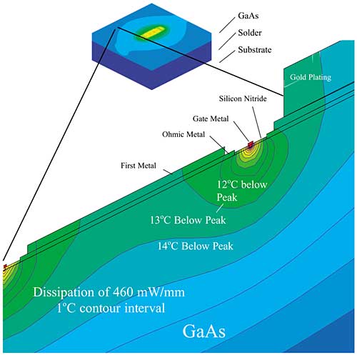 |
Figure 3. Example of thermal model temperature contours.An example of a FET thermal model temperature contour is shown in Figure 3. This figure illustrates the strong temperature gradients near the FET channels. This model was generated by continually refining the mesh in regions of high temperature gradient. The large spatial scale range required to model the device is also shown by comparing the zoomed-in portion of the FET channels to the overall dimensions of the MMIC. The MMIC dimensions are in thousands of microns while the gate length is less than one micron. An alternative technique to continual mesh refinement is to apply temperature boundary conditions from coarser models to finer models. In this approach, the substrate, die attach and a coarse representation of the FET are modeled to supply temperature boundary conditions to a finer meshed model that resolves the channel region.
Design Considerations
Thermal engineers often spend considerable effort designing system cooling techniques where adding forced convection or a better heatsink will reduce the system temperature a few tens of degrees. Because so much of the total temperature rise from the junction to ambient for GaAs FETs is within the GaAs, it is instructive to consider the thermal impact of various FET designs. While many FETs are already designed and the thermal engineer does not have influence over their use, the advantages of considering the complete thermal picture are obvious.
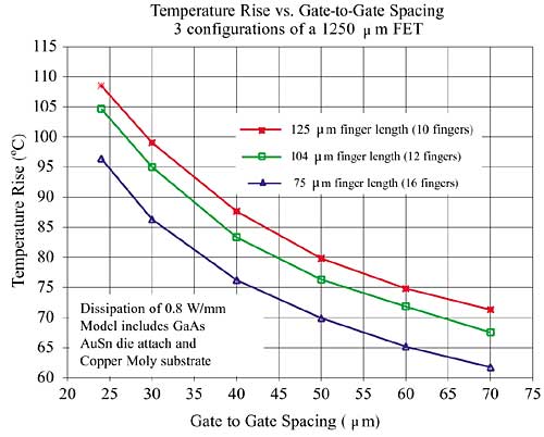 |
Figure 4. Temperature rise as a function of gate spacing.Figure 4 illustrates a design trade for a 1250 �m FET comparing three potential FET layouts. Each of the three layouts has a 1250 �m periphery (10 x 125, 12 x 104, and 16 x 75 �m). The choice of FET layout involves more than just thermal considerations but notice that temperature reductions on the order of 10 to 20oC are possible. For example, the 16 x 75 �m layout is 10oC cooler than the 10 x 125 �m at a constant 50 mm gate-to-gate spacing. Alternatively, reducing the gate-to-gate spacing from 38 to 50 �m for the 10 x 125 �m FET reduced the junction temperature by 10oC.
Achieving a comparable temperature reduction with a fan or heatsink may be more expensive and complicated than working the thermal issues from the very beginning. It should be noted that increasing the gate-to-gate spacing increases the device cost because fewer devices can be processed per wafer. Phased array radars often have antenna grid spacing limits that force the FET gates to be placed closer together. The main point from Figure 4 is to show that thermal design focused at the FET level can have more payback than determining how to cool the package later.
Transient Considerations
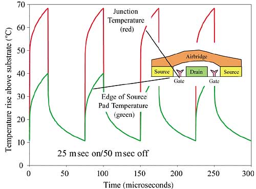 |
Figure 5. Junction and pad temperatures in a pulsed application.Power amplifiers are often operated in a pulsed manner, especially in radar systems. The range of pulse widths is from on the order of one microsecond to several milliseconds. Figure 5 shows the junction temperature response of a GaAs FET subjected to a pulsed profile consisting of 25 �sec on and 50 �sec off. The plot shows the quasi steady-state response after many pulses. Notice that the time constant for the junction is on the order of one msec (the red line is the junction temperature). The plot also illustrates the response at the source pad near the junction (the green line) and shows that the temperature swing is significantly less than at the junction.
In fact, for this case, the temperature swing will be very small at the base of the GaAs, and it would be appropriate to use a time-averaged power for a system level thermal model. Computing results such as these requires significant computation time, and techniques have been developed to significantly reduce the computer time requirement [8]. Transient modeling of GaAs FETs requires accurate treatment of the large temporal scale range, which ranges from fractions of a microsecond at the junction to tens or hundreds of milliseconds at the device level.
Conclusions
Thermal analysis of GaAs FETs requires understanding features at the semiconductor level. A brief summary of techniques to predict the temperature field within the GaAs has been given to assist the thermal engineer with the choice of analysis methods. It is hoped that this brief overview of some of the thermal issues associated with GaAs FETs will provide some insight into the modeling complexity and the need for grid convergence studies during numerical modeling. It should be noted that these same issues apply to future high frequency semiconductors such as gallium nitride. Job security for thermal engineers seems to be intact because these future semiconductors are capable of heat dissipation levels at least five times greater than GaAs devices.
References
- Wilson, J. and Decker, K., “GaAs MMIC Thermal Modeling for Channel Temperatures in Accelerated Life Test Fixtures and Microwave Modules,” Proceedings, SEMI-THERM X, San Jose, March 1994.
- DeLorenzo, et al, “GaAs FET Principles and Technology,” Artech House, 1982.
- Kopp, B., Ouellette, E., and Billups, A., “Thermal Design Considerations for Wide Bandgap Transistors,” Microwave Journal, June 2000.
- Kokkas, A.G., “Analysis and Design of Electrothermal Integrated Circuits,” Ph.D. Thesis, MIT, 1972.
- Albers, J., “An Exact Solution of the Steady State Surface Temperature for General Multilayer Structure,” Proceedings, SEMI-THERM X, San Jose, March 1994.
- Dawson, D., “Thermal Modeling, Measurements and Design Considerations of GaAs Microwave Devices,” Proceedings, IEEE GaAs IC Symposium, Cleveland, 1994.
- Cindas Semiconductor Properties Report, Purdue University, 1988.
- Wilson, J. S., Raad, P.E., and Price, D.C., “Transient Adaptive Thermal Simulation of Microwave Integrated Circuits,” Proceedings, SEMI-THERM XIV, San Diego, March 1998.


