What information does light, reflected from a running electronic device, carry? Our research team has been working upon this key question for almost a decade. As this magazine is dedicated to thermal issues, we will focus upon these aspects of optical probing.
Figure 1 shows the general principle of our experimental method. Light is shone upon a running device. When the device under test is operated, reflection (due to light-material interaction) modifies the properties of the outgoing light wave relative to the incoming one.
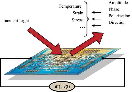 |
Figure 1. General principle of the experimental method of optical characterization.Light can be characterized, among other things, by its amplitude, phase, polarization, direction, and divergence. All of these parameters can carry information related to physical phenomena occurring within the device. Temperature changes, thermal expansion with its induced effects of deformation, and stress are examples of phenomena that modify the properties of reflected light and therefore apply a signature on the light beam.
The basic objectives of our experimental method are as follows:
- To identify, as accurately as possible, the incoming light beam properties in terms of the above-mentioned characteristics
- To build very sensitive optical instrumentation that enables us to select a given action on the outgoing light, which is induced by running the device or component under test.
We use high-quality laser beams and self-built, dedicated optical instruments. The link between the measured quantities and a physical model of the interaction provides valuable data concerning the device under test. As our approach is based upon changes induced by the operating device, we need to observe time-dependent phenomena; for example, on-off responses or sine wave excitation.
Temperature Measurement through Reflectance Changes
The reflectance of the materials (R) involved in electronic devices, such as metals and semiconductors, is temperature dependent. The reflectance variations (R) relative to temperature changes (
T) are of the order of 10-4 – 10-5 per oC for visible light wavelengths. These very small values allow writing the relative reflectance change as linearly related to the temperature variation
T:
Provided is known, the measurement of the relative reflectance change provides a direct absolute value of
T. This very simple and straightforward measuring method, known for many years [1-4], must be handled with care, as coefficient
is equipment dependent in most situations. The use of high focusing microscope objectives allows us to measure the temperature variation on surfaces as small as 0.5 mm in diameter.The measurement of the calibration factor
, especially under high focusing conditions, necessitates the use of particular measuring procedures, which we have developed recently.Figure 2a shows a schematic view of our reflectance set-up in which a device is mounted upon a temperature-controlled bench. A piezo-actuator keeps the distance focus-sample constant. Figure 2b shows the temperature response of the control temperature together with the reflectance response. The constant ratio between signals is the instrumental calibration coefficient. Because this coefficient is determined in-situ, the reflectance set-up can measure absolute temperature changes due to the operating device. This system serves as a high-resolution (0.5 �m), fast (125 MHz), and sensitive (< 0.0001oC) absolute thermometer for measuring temperature changes on electronic and microelectronic equipment.
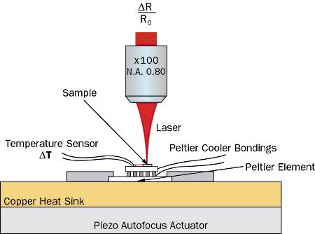 |
Figure 2a. Temperature controlled optical reflectance bench, allowing calibration of the reflectance temperature measurements of electronic devices.
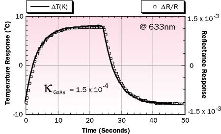 |
Figure 2b. Simultaneous temperature control and reflectance response, as a function of time, upon an IC surface.
Surface Displacement Measurement through Light Phase Changes
Surface displacement, due to thermal expansion for example, will induce phase changes upon the reflected light. The knowledge of surface displacement can be essential in terms of device reliability. This is particularly true when validating computer simulation thermal expansion programs and using them to evaluate failure risks. Optical instruments can measure very small surface displacements with extreme accuracy. We will distinguish below between point measurements and whole surface analysis (which we call displacement imaging).
Point Measurement
Using laser interference techniques, we can perform out of plane surface displacement very accurately. We have developed a very high resolution Michelson interferometer for electronic device and circuit analysis [5,6]. Such devices utilize a single detector, i.e., a photodiode recording the intensity of the interfering outgoing beams.
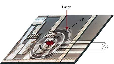 |
Figure 3a. Partial view of an IC indicating where laser probing was performed. Transistor T has a sine wave table.Figure 3a shows part of an IC board, illustrating some transistors. Upon application of AC power to transistor T at frequency w, a surface displacement at 2w occurs on top of it due to the power released PT(2w)in the transistor by Joule effect:
where IT(w) is the drain current flow into the transistor and VT(w) the drain-source voltage. The released heat diffuses from the source T into the chip. A surface temperature field T(x, y, 2w) is created around transistor T. A coupling between temperature and expansion occurs, inducing a surface normal displacement z (x, y, 2w ) around source T(x=0, y=0, 2w).Figure 3b shows the surface normal displacement amplitude as a function of injected current and measured at a point near the source. We observed a pure quadratic response, indicating a well-known thermal effect: Joule heating. Harmonic surface displacements at 2w of 10-15 m can be measured, which means the bench can detect normal surface displacement with better than femtometer sensitivity.
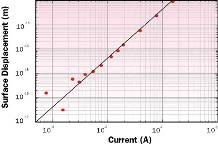 |
Figure 3b. Periodic surface displacement amplitude as a function of current in transistor T. Amplitudes as low as a few femtometers can be measured.It is important to remember that interferometry displacement measurements are absolute as referenced to the light wavelength through phase changes. This very sensitive instrumentation allows us to detect and to follow very tiny thermal phenomena on electronic devices. We have, for example, measured Peltier effects in integrated circuits at metal-semiconductor junctions [5, 7].
Based on measurements of very small surface displacements on running integrated circuits, we have identified the following astonishing results: “breathing” of the components due to their thermal activity, and propagation of surface waves around these heat sources. Comparable to seismic waves on the earth, the thermal waves can be used to detect the sources [8,9,10]. Of course, high-resolution interferometry is needed, coupled to a lock-in detection, to measure the in-phase and out-of-phase component of the signal. From this the surface displacement can be derived (Figure 3b). The method allows us to reach the shot noise limit, which is the noise due to the quantum aspect of light. This is the noise limit of the detector.
Imaging Techniques
Instead of concentrating a laser beam spot onto a small area, imaging interferometry uses a laser beam to cover the entire device surface being analyzed. And, instead of a single photodiode, a CCD camera records the useful information. The device and camera are configured in an object-image optical set-up. Each pixel of the CCD becomes an interferometer by combining, on the CCD detector, the device image and a plane surface reference image.
When the object point of a given image pixel moves in the direction of observation, a phase change of the image occurs. This phase change is recorded through the interference with the reference beam. An extraction procedure together with a calibration allows absolute values for the displacement of each surface point to be obtained [11,12].
Figure 4 shows the surface displacement of a standard Peltier cooling device (typical size 25 x 25 mm) when a 1oC temperature difference is applied between opposite faces. With this method, displacements in the nanometer scale can be observed.
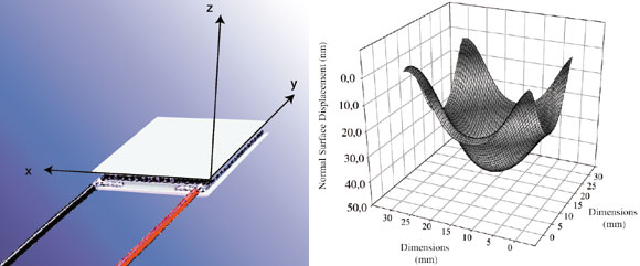 |
Figure 4. Surface deformation of a Peltier cooling element measured by imaging interferometry when a temperature difference of 1oC is applied between faces.When the illumination and observation directions coincide as in a Michelson set-up, surface displacement in this direction can be measured. But when these two directions differ, it is possible to measure in-plane displacements. This means imaging interferometry provides a means to measure the three displacement components (u, v, w) of any given point (x, y, z) of a device’s surface. This is very powerful as it provides all the information about surface displacement one can get from a non-contact, non-destructive analysis of a running device.
Moreover, we have developed an experimental set-up, called shearography [13], which allows us to measure, via an imaging method, most of the spatial derivatives (i.e., u/
x,
u/
y,
v/
x,
v/
y,�) of any surface point displacement component.This is done with a set-up by which interferences of two spatially displaced (
x or
y) images of the device under test are recorded on the CCD camera. From this it is possible to estimate a useful quantity in terms of mechanical reliability: the deformation energy [14]. The deformation energy is a fragility indicator, giving a good view of the regions where mechanical failure will most likely occur. Figure 5b shows the power transistor studied with the shearography imaging method developed in the lab. Figure 5a shows the deformation energy determined for the transistor under normal functioning conditions.
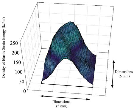 |
Figure 5a. Deformation energy determined from shearography imaging of a power transistor under normal operating conditions.
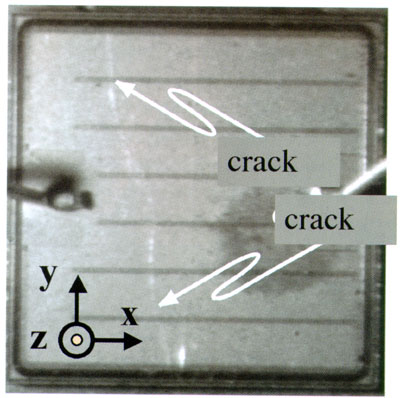 |
Figure 5b. View of the power transistor after a lethal power increase was applied. A crack is clearly seen along the maximum deformation energy.The maximum deformation energy localizes the regions where highest stress is applied and where mechanical failure has the highest probability. Figure 5b shows a view of the power transistor after a lethal failure was obtained by increasing the injected power. A crack is clearly seen following the direction of highest deformation energy.
Conclusion
Optics in general and laser optics in particular provide new ways to explore thermal issues in electronics. Original temperature measurements with high sensitivity, high spatial resolution, and fast response can be performed. Imaging set-ups based on interferometry provide new tools to tackle reliability issues in terms of mechanical failure.
References
- Rosencwaig, A., Opsal, J., Smith, W., and Willenborg, D., “Detection of Thermal Waves through Optical Reflectance”, Applied Physics Letters 46, 1985, p 1013.
- Voigt, P., Hartmann, J., and Reichling, M. “Thermal Wave Imaging of Electrically Heated Microstructures”, Journal of Applied Physics, Vol. 80, No. 4, 1996, pp 2013-2018.
- Phan, T., Dilhaire, S., Quintard, V., Lewis, D., and Claeys, W., “Thermoreflectance Measurements of Transient Temperature upon Integrated Circuits: Application to Thermal Conductivity Identification”, Microelectronics Journal, vol 29, Nos 4-5, 1998, pp 170-180.
- Quintard, V., Dilhaire, S., Rauzan, C., Phan, T., and Claeys, W., “Measurement of Absolute Temperatures upon Metallic Lines under Current Stress by Laser Probing”, IEEE Transactions on Instrumentation and Measurement, Vol. 48, No. 01, 1999, p 69.
- Claeys, W., Dilhaire, S., Quintard, V., Lewis, D., Phan, T., and Aucouturier, J., “Optical Ammeter for Integrated Circuit Characterization and Failure Analysis”, Quality and Reliability Engineering International, Vol. 11, 1995, pp 247-251.
- Claeys, W., Dilhaire, S., Jorez, S. and Patino Lopez, L., “Laser Probes for the Thermal and Thermomechanical Characterization of Microelectronic Devices”, Microelectronics Journal, 32, 2001, pp 891-898.
- Deboy, G., S�lkner, G., Wolfgang, E. and Claeys, W., “Absolute Measurement of Transient Carrier Concentration and Temperature Gradients in Power Semiconductor Devices by Internal Deflection Spectroscopy”, Microelectronic Engineering, 31, 1996, pp 299-307.
- Dilhaire, S., Schaub, E., Claeys, W., Altet, J., Rubio, A., “Localization of Heat Sources in Electronicrcuits by Microthermal Laser Probing”, International Journal Thermal Science, 39, 2000, pp 544-549.
- Altet, J., Rubio, A., Schaub, E., Dilhaire, S., and Claeys, W., “Thermal Coupling in Integrated Circuits: Application to Thermal Testing”, IEEE Journal of Solid-State Circuits, 36, 2001, pp 81-91.
- Altet, J., Dilhaire, S., Grauby, S., and Volz, S., “Advanced Techniques for IC Surface Temperature Measurement”, ElectronicsCooling Vol. 8, No. 1, 2002, pp 22-28.
- Nassim, K., Joannes, L., Cornet, A., Dilhaire, S., Schaub, E., and Claeys, W., “Thermomechanical Deformation Imaging of Power Devices by Electronic Speckle Pattern Interferometry”, Microelectronics Reliability, Vol. 38, 1998, pp 1341-1345.
- Dilhaire, S., Jorez, S., Cornet, A., Schaub, E., and Claeys, W., “Optical Method for the Measurement of the Thermomechanical Behaviour of Running Electronic Devices”, Microelectronics Reliability, Vol. 39, 1999, pp 981-985.
- Hung, Y., and Liang, C., “Image-Shearing Camera for Direct Measurement Of Surface Strain”, Applied Optics, Vol. 18, No.7, 1979, pp 1046-1051.
- Dilhaire, S., Jorez, S., Patino Lopez, L., and Claeys, W., “Measurement of the Thermomechanical Strain of Electronic Devices by Shearography”, Microelectronics Reliability, 40, 2000, 1509-1514.


