Thermal and EMC design in high-speed digital electronics systems has become a battle of conflicting requirements. Faster switching has led to increased electromagnetic (EM) emissions due to the extended bandwidth of signals. Higher-density components are consuming more power, generating increased EM fields and more heat.
Electronics equipment must comply with radiation limits set by the Federal Communications Commission (FCC) [1]. Careful design of the board layout is necessary to minimize the sources of radiation. However, it is impossible to eradicate all EM fields at the board level. Cables are often the most significant contributors to the EM emissions. If the board is shielded by an enclosure, there is danger of a design conflict: Thermal design requires perforations to enable airflow, whereas EMC design requires a “watertight” enclosure to prevent EM emissions. If frequencies are high, wavelengths will be similar to aperture dimensions and resonance will occur, exasperating the EMC problem.
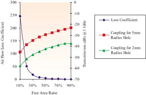 |
Figure 1. Thermal and EM air vent characteristics.Figure 1 plots the airflow loss coefficient (for highly turbulent flow) and the EM transmission across a vent. A small free area ratio (FAR) of less than 30% has a dramatic effect on pressure drop. Increasing the FAR increases the EM transmission across the panel and for a given FAR, it is better to have many small holes rather than few large holes.
Integrated Thermal/EM modeling enables design conflicts to be quickly identified and visualized. In this article we apply this approach to an Intel Pentium®-100 PC. The computer has long been in the market, satisfies thermal constraints and complies with FCC limits. The P100 is relatively low speed and power by today’s standards. However, we imagine that the system requires a processor upgrade. This raises the question; is there sufficient margin in the thermal and EMC design without a change in architecture?
Baseline Model Details
The computer was tested for EM emissions and temperatures at a compliance laboratory [2].
Thermal Model
The model was defined using commercially available CFD software [3]. Adequate boundary conditions were specified to match the test environment. Figure 2 shows an interior view. The chassis, constructed from mild steel, is 431.8 mm x 406.4 mm x 152.4 mm (17″x16″x6″). The motherboard supports various cards such as modem, joystick and networking. These cards were not active during the tests and did not dissipate heat, but were allowed to conduct. The graphics board was assumed to dissipate approximately 2 W. The model represents blockages due to the connectors and RAM.
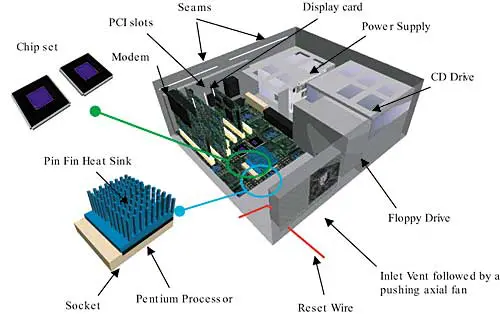 |
Figure 2. Pentium PC description.The chip set was constructed using two plastic quad flat packages (PQFP), each package dissipating 1 W of power. A DELPHI compact model of the PQFP [2] provided an equivalent set of thermal resistances. Out of the many advantages of a DELPHI compact model, one can retain the boundary condition independence.
The processor, a cavity-down ceramic pin grid array, was modeled in detail. The power dissipation was assumed to be the maximum power of 10 W since the PC was running intense calculations during the experiments. Other components dissipate a total of 20 W, which is typical for this type of board. The remaining parts, such as the floppy disk, CD and hard drive block the flow, but do not dissipate. A power supply, cooled by an axial fan, extracts air out of the chassis. An additional axial fan, facing the pin fin heat sink, provides air to the motherboard. Ambient air temperature was measured at 24.5oC for the duration of the experiments.
EMC Model
The mechanical aspects are inherited from the thermal model. EM attributes are attached and wires/apertures added. A wire passes through the front of the enclosure to a reset switch on a plastic face panel. A metal cage on the back of the face panel contacts the enclosure when screwed together. This forms an EMI shield around the reset wire.
The system was deliberately tested and modeled with the front panel open to investigate both conducted and radiated emissions. The inlet vent has 2 mm radius holes and 1 mm metal thickness. At the back of the PC the lid overlaps the rear panel by 1cm and is screwed to the chassis in both corners and the center. This creates two 17 cm long seams. The model treats these as worst-case; i.e., no electrical contact along their length. There are 14 PCI slots each 9.8 cm long with a 0.5 mm gap width.
Near-field probes were used to scan over the motherboard and search for EM “hot spots”. Surprisingly, very little field could be detected around the traces, but the fields were intense around the ICs. Trace fields are generally cancelled by their images in the ground plane. The images of IC pins are additive. In the EM model voltage pulses are attached to short wires between each IC and the ground plane. The spectrum is constant with frequency, enabling broadband emissions to be extracted from a single computation.
Thermal Baseline Results
A thermocouple was connected to the top surface of the heat sink base to measure temperature. The measured temperature was 51.7oC and the baseline simulation gave 53oC. Figure 3 displays the simulated surface temperature distribution on the heat sink. The junction temperature in the CBGA die is 59oC, which is below the design constraint of 85oC.
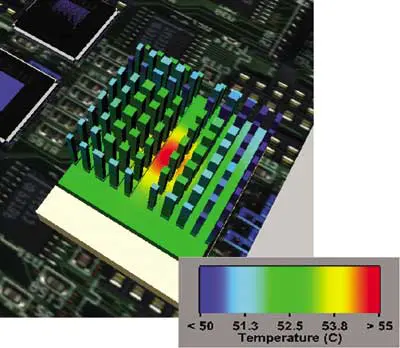 |
Figure 3. Surface temperature of the heat sink.
EMC Baseline Results
Electric and magnetic fields are sampled inside the enclosure and 3 m away. Figure 4 shows the radiated electric field around the PC. The radiation peaks at 133, 390, 825 and 900 MHz. This spectrum reveals the continuous broadband response of the PC. The actual PC generates discrete frequencies derived from clock frequencies and their harmonics. The Intel developer’s guide [4] provides electrical data for the Pentium Processor. The specifications for the P100 are 33 MHz clock and 0.15 nS to 1.5 nS rise/fall times.
In Figure 4, the broadband spectrum is multiplied by the clock spectrum in the simulation. The results are compared with test data taken in an anechoic chamber [3]. The emissions are virtually within FCC Class B limits (46 dB�V/m between 216 MHz and 960 MHz), despite the reset wire being unshielded. The simulation exaggerates emissions above 700 MHz since there is no electrical contact along the seam in the model.
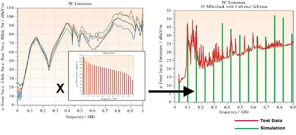 |
Figure 4. Impulse spectrum and corresponding digital spectrum.EM modeling enables surface currents and fields to be visualized. This is valuable for determining why emissions peak at certain frequencies as shown in Figure 5.
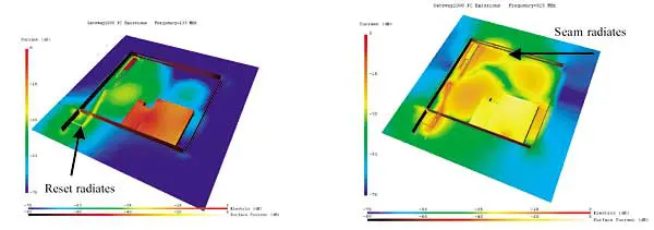 |
Figure 5. Current and electric field distributions at 133 and 825 MHz.The EMC simulation provides a cylindrical scan around the system on a 3 m radius, mimicking the FCC EMC test standard. The scan in Figure 6 shows high vertically polarized radiation, suggesting that the seams are the culprits.
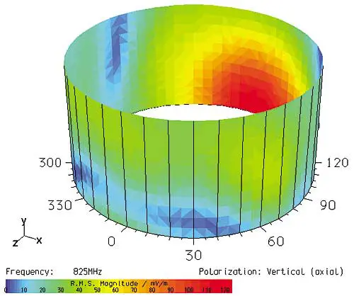 |
Figure 6. Simulated cylinder scan around PC at 825 MHz.
Hypothesized Upgrade
The P100 processor is to be replaced by a new IC having twice the clock frequency, half the rise/fall time and twice the power consumption.
On the thermal side, we would be concerned about the increase in junction temperature, since the device is now operating at 20 W. The chip set power levels will correspondingly increase to 2 W per chip. The results in Figure 7 show an increase in junction temperature to 81oC, which is too close to the limit (85oC). A similar behavior can be noticed for the chip set, which has a junction temperature equal to the design constraint (100oC). The EMC results in Figure 8 show that the emissions have increased, most noticeably above 700 MHz, where the field now exceeds 65 dB�V/m.
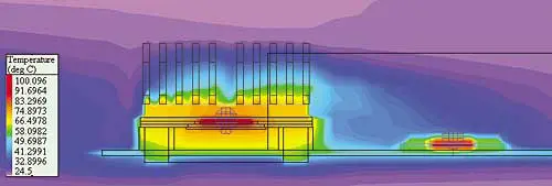 |
Figure 7. Temperature profile for upgraded system.
 |
Figure 8. Simulated radiated emissions for baseline and upgraded system.There is a risk that the existing design will be inadequate from both thermal and EMC points of view. The thermal design could be improved by using a new heat sink with a larger surface area, but it may come at a price and worsen EM issues. Heat sinks can potentially behave like antennas where the resonant frequency depends on the physical size. We could increase the free area ratio of the inlet vent but this will worsen electromagnetic emissions.
To improve the EMC design, we could utilize EMI gaskets in the seams and apply ferrite or bypass capacitor filters to the reset wire. This would not benefit the thermal design. Perhaps we could place an EMI shield over the processor and chip set, but it is not obvious how this will affect thermal performance. If we perforate the top and sides of the shield air will be able to filter through (Figure 9). It’s worth investigating!
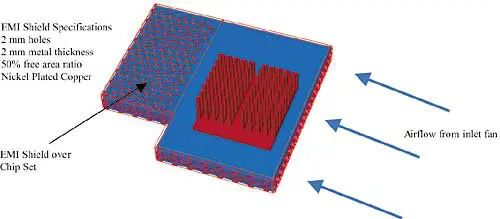 |
Figure 9. Simulated EMI shield over processor and chip set.
|
Table 1. Simulated Upgrade and EMI Shielding Thermal ResultsNumerical results in Table 1 show a slight increase in the chip-set junction temperature, which exceeds the design constraint. On the other hand, the processor temperature has decreased, mainly because the EMI shield offers an additional path for the heat conducting from the processor to the heat sink. The chip set does not benefit from the new conduction path since it is not in contact with the shield. It would be interesting to introduce a conduction path using a piece of nickel-plated copper, to see if that would improve heat dissipation. The perforations in the EMI shield directly above the chip set are closed. Surprisingly, the results in Table 1 reveal that the chip set junction temperature is worse! The processor heat spreads into the shield and heats the chip set. Furthermore, there is insufficient convection above and around the EMI.
The EM results in Figure 10 show a significant reduction in radiated emissions. This model assumes continuous electrical contact between the sidewalls of the shield and the motherboard ground plane. This is the “best case” situation. The model could be refined to examine the effect of non-continuous grounding and to determine the optimal ground points.
 |
Figure 10. Radiated emissions with processor and chip set shield.The EMC design has plenty of margin and the requirements could be relaxed to give more design space to the thermal engineer. Perhaps a more efficient heat sink could be placed on the EMI shield to bring the thermal design into specification. Since the heat sink is grounded through the EMI shield, we may be able to avoid EM resonant behavior. We leave you to speculate.
Conclusions
This article has demonstrated the thermal/EMC conflict that is typical of electronics design today. We have investigated the EM emissions and thermal performance of a Pentium PC. By hypothesizing a processor upgrade, we have shown just how challenging thermal and EMC design can be. Integrated thermal and EMC modeling helps engineers explore design options quickly and ultimately helps reduce the risk of equipment over heating and failing compliance tests.
References
- Code of Federal Regulations, Title 47, Part 15, Subpart B: “Unintentional Radiators”.
- Curtis-Strauss Compliance Laboratories located in Littleton MA, USA.
- Flomerics FLOTHERM®, FLOPACK™ and FLOEMC™ software.
- Intel Pentium® Processor Family Developer’s Manual.


