Warpage of FC-PBGA Packages
Flip chip technology has emerged as an important chip-level package solution to meet the ever-increasing demand of high I/O requirements. The flip chip technology was implemented originally for a multi-layer ceramic substrate. In the ceramic flip chip package, a shear strain in each bump, produced by the mismatch of the coefficient of thermal expansion (CTE) between the chip and the ceramic substrate, is proportional to its distance from the neutral point (DNP). Consequently, the size of the silicon device is limited to prevent solder bumps from premature failure. In recent years, an innovative underfill technique was developed and implemented for the flip chip technology to enhance solder bump reliability, where the gaps between the solder bumps are filled with an epoxy encapsulant. The remarkable improvement of solder fatigue provided by the underfill has enabled the industry to extend the flip chip technology to organic substrates, leading to the development of the flip-chip plastic ball grid array (FC-PBGA) package.
While the underfill reduced thermo-mechanical deformations of solder bumps, the global bending deformations of packages were much more exacerbated because of the higher CTE of organic substrates and a higher degree of coupling through the underfill. Several whole-field optical methods have been employed for warpage measurement of electronics components [1]. They include Twyman/Green (T/G) interferometry and shadow moir�. Although simple, the application of T/G interferometry is limited since it requires a specular (mirror-like) surface [1,2]. In addition, its measurement sensitivity is a fraction of micron, which is usually too high for typical warpage observed in the flip-chip packages. Shadow moir� provides a sensitivity of 25 to 50 microns and it has been used extensively to measure the warpage of PCBs [2,3]. With the method, a small distance between the specimen and the reference grating is required for fringe formation; consequently, the chip and the substrate cannot be viewed simultaneously. In addition, a diffusive surface is required for good fringe visibility; this is typically done by spraying a white matte paint and it is not desired for nondestructive testing. These inherent limitations of shadow moir� make it impractical for the flip-chip packages.
For FC-PBGA package applications, the measurement sensitivity in the range of microns is ideal. A large tolerance in specimen surface roughness is required to test the ground surface of the chip and the organic substrate without any specimen preparation. The warpage is to be measured as a function of temperature to simulate operating and accelerated testing conditions. These technical requirements were the immediate motivation for the development of far infrared Fizeau interferometry (FIFI). The following section describes the technique as a tool to characterize the warpage behavior of FC-PBGA package.
Far Infrared Fizeau Interferometry
It has been known that the specular component of the reflected light (mirror-like reflection) increases as the wavelength or the angle of incidence increases. Consequently, with a longer wavelength, a surface regarded as optically rough under visible light can be treated as a specular surface. The increase of specular reflection can be explained qualitatively by using the definition of effective roughness, R, known as “Rayleigh criterion”
 |
where h=Height of surface irregularities
=Wavelength
=Angle of incidence
Theoretically, a surface will become perfectly smooth when h/ approaches zero or
approaches 90o.
Fizeau interferometry is a classical interferometry using visible light, which measures the surface topography of a slightly warped specular surface. Far infrared Fizeau interferometry extends the domain of its application by employing light with a very long wavelength and thus decreasing the effective roughness of specimen surface [4]. Considering = 10.6 �m for a CO2 laser, the effective roughness is reduced by a factor of 20 for a given angle of incidence, compared with a wavelength in the middle of visible spectrum (green light at 0.5 �m). Consequently, optically rough surfaces, such as the ground surface of silicon, organic substrate, etc., can be tested without any specimen preparation.
 |
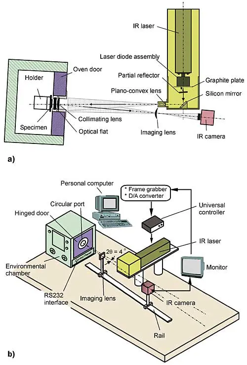
Figure 1. (a) Optical and (b) mechanical configuration of FIFI for real-time observation.
The optical configuration of FIFI is explained in Figure 1a [4]. The beam from the laser is first divided by a partial reflector to reduce the intensity. The transmitted light is expanded and is subsequently collimated by a collimating lens. An optical flat is placed next to the collimating lens. The optical axis of the collimating lens is perpendicular to the optical flat and the expanded beam illuminates them with a small angle of incidence. A portion of the collimated beam is reflected from the optical flat while the transmitted beam is reflected from the specimen surface. The reflected beams are collected by an infrared CCD camera.
The wavefront from the optical flat, which is originally flat, interferes with the wavefront from the specimen to produce a contour map of the z coordinate of the surface. The W displacement can then be determined by
 |
where N = Fringe order at each point in fringe pattern
=Angle of incidence
=Wavelength of laser light employed
With a small angle used in the system (cos
1), the measurement sensitivity is defined as
/2 per fringe order (5.3 �m per fringe order).
The mechanical configuration for real-time observation is illustrated in Figure 1b [4]. An air-cooled CO2 laser is used as a coherent light source. An expanded beam illuminates the optical flat and the collimator mounted on a specially designed port of an environmental chamber. The chamber has a heating/cooling rate of 0.5oC/sec. and its operating temperature range is -40 to 300oC. The imaging system is comprised of an imaging lens and an infrared CCD camera. The imaging lens is mounted on a translation stage that travels along a rail to provide a desired magnification factor for various sizes of specimens. The image is displayed on a monitor and the output from the monitor is digitized by a frame grabber for image processing.
Characterization of FC-PBGA Package Behavior
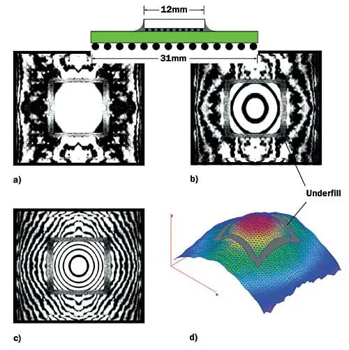
The warpage behavior of an FC-PBGA package was evaluated by FIFI. The cross sectional view of the package is shown in Figure 2. A square chip (12 x 12 mm) was mounted on a BT based substrate (31 x 31 mm). Initially, the package was heated to an underfill curing temperature (150oC). Then, the deformations of the top surface of the package were documented while cooling the package to room temperature. The fringe patterns obtained at 150oC, 100oC and room temperature are shown in Figure 2a-c, where the contour interval is 5.3 �m per fringe order. The package was virtually flat (devoid of fringes) at the underfill curing temperature. The large mismatch in CTE caused the package to bend as the temperature decreased.
 |
Figure 2. Warpage contours of FC-PBGA package documented at (a) 150oC, (b) 100oC and (c) room temperature, where the contour interval is 5.3 �m per fringe order. A 3-D warpage map at room temperature obtained by digital image processing is shown in (d).
It is important to note that the fringe patterns from the chip and the substrate were recorded from a single experiment although the surfaces of the silicon and the substrate were not located in the same plane. In addition, the high signal-to-noise ratio provided by the fringes on the rough surfaces of the chip and the substrate clearly indicates highly effective roughness tolerance of the method.
A 3-dimensional representation of the warpage at room temperature is shown in Figure 2d, which reveals a significant bending in both chip and substrate. Irregularities shown in the substrate are not caused by optical noise. Instead, they represent the heterogeneous deformation of the multi-ply glass/epoxy composite.
Thermal Solutions for Flip Chip Packages
With flip chip technology, the conventional orientation of the chip is reversed. The chip is placed face downward and the connection between the chip and the chip carrier is achieved by solder bumps. Because of this new orientation, the top surface of the chip is available for enhanced thermal management solutions.
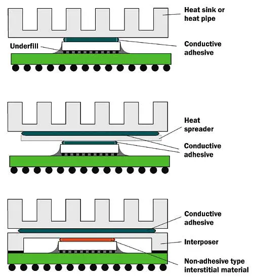
Figure 3 illustrates thermal solutions uniquely available for flip-chip packages. The first two solutions involve direct attachment of a heat sink with or without a heat spreader. They are suitable for adhesive type interstitial materials. These materials are typically low modulus adhesives filled with thermally conductive particles. The bulk thermal conductivity of typical conductive adhesives is less than 1W/mK and thus the solutions are more suitable for relatively low power applications.
 |
Figure 3. Thermal management solutions uniquely available for FC-PBGA packages.
The third solution, called an interposer or cap configuration, was introduced to cope with the above problem and has been applied successfully for many high performance flip chip packages. In the configuration, an interposer was present between the chip and the heat sink, which allowed use of non-adhesive type interstitial materials with higher thermal conductivity, such as thermal grease, thermal gel, elastomeric gaskets, phase change materials, etc. This configuration has become progressively more important as power densities increase rapidly due to the miniaturization of device line features.
The inherently large warpage of FC-PBGA packages described in the previous section poses a new technical challenge in the high performance thermal solution, i.e., non-uniform thermal conductance at the chip/interposer interface.
Effect of Warpage on Thermal Interface
When the chip is powered and thus the device is subjected to a temperature excursion, each material expands at a different rate. This non-uniform CTE distribution produces thermally induced warpage in the chip and substrate. Consequently, the gap between the chip and the interposer changes repeatedly under device operating conditions (power cycling), as illustrated in Figure 4.

If a non-solid interstitial material such as thermal grease or gel is used, the gap change reduces the volume of the material. The material is gradually squeezed out during the repeated power cycling and eventually causes significant degradation of thermal performance; this phenomenon is known as “pump-out” [5,6].
Recently, Chiu et al. conducted a systematic investigation on the pump-out behavior [6]. In their test vehicles, the interposer was connected to the substrate to produce a gap with approximately 0.25 mm between the interposer and the chip, and the gap was filled with a silicon-oil based AlN filled thermal grease. The package assembly was subjected to a power cycling condition. The results confirmed that the failure mechanism of thermal interface was dominated by the grease pump-out. For the regions with active grease pump-out, the majority of thermal grease was squeezed out and only some silicone oil remained.
It is important to note that the volume change during power cycling is directly proportional to a change in the total warpage of the package since the interposer is mechanically connected to the substrate. For the fringe patterns shown in Figure 2, the warpage change of the package, caused by cooling it from 100oC to room temperature, can be determined using Equation 2. The warpage changes in the chip and the substrate were 21.2 �m and 23.90 �m, respectively. If the package were used for the interposer design, the total warpage change that would contribute to the change in the gap would be 45.1 �m. This would reduce the original volume of thermal grease or gel significantly and it should be considered in the design of a thermal solution.
If a solid interstitial material, such as an elastomeric gasket or phase change material, is used at the thermal interface, the effect of warpage becomes more serious. The joint thermal conductance of a metal/polymer interface, hj, can be defined as [7,8]
 |
where hmicro,1 and 2 are the microscopic contact conductance at the polymer/interposer and polymer/chip interfaces, respectively, and hbulk is the bulk thermal conductance of a polymer layer. The microscopic contact conductance and the bulk thermal conductance can be expressed as [8]
 |
|
The micro contact conductance and the bulk thermal conductance are functions of the apparent pressure. The apparent pressure during power cycling is governed by the initial pressure, Pi, that is applied at the assembly process and the gap change between the chip and the interposer. The gap change caused by the warpage varies over the chip and it produces a non-uniform distribution of the apparent interface pressure. The pressure non-uniformity results in a significant variation in thermal conductance over the chip/polymer interface [8]. The initial pressure must be determined carefully to avoid hot spots during operation after considering a pressure drop/increase caused by the warpage.
Summary
High performance thermal solutions uniquely available for FC-PBGA packages were reviewed. The warpage characteristic was identified as an important design parameter in achieving optimum mechanical/thermal solutions for high performance FC-PBGA packages. A critical technical challenge associated with its warpage was discussed. An interferometric technique utilizing far infrared light was introduced as a tool to characterize the warpage of packages without any specimen preparation. The technique is ideally suited to FC-PBGA package applications and the results can be used to assess the performance of thermal interfaces with non-adhesive type interstitial materials.
References
- Han, B. and Guo, Y., “Photomechanics Tools as Applied to Electronic Packaging Product Development,” Experimental/Numerical Mechanics in Electronics Packaging, Vol. 1, (Han, B., Mahajan, R., and Barker, D., ed.), Society for Experimental Mechanics, Bethel, CT, April 1997.
- Post, D., Han, B. and Ifju, P., “High Sensitivity Moir�: Experimental Analysis for Mechanics and Materials”, Springer-Verlag, New York, 1994. Also Post, D., Han, B. and Ifju, P., “Moir� Methods for Engineering and Science – Moir� Interferometry and Shadow Moir�,” Chap. 7, Photomechanics for Engineers, (Pramod Rastogi, ed.), Springer-Verlag, 2000.
- Stiteler, M. and Ume, I. C., “System for Real-Time Measurement of Thermally Induced Warpage in a Simulated Infrared Soldering Environment,” Journal of Electronic Packaging, Vol. 119, pp. 1-7. 1997.
- Verma, K. and Han, B., “Warpage Measurement on Dielectric Rough Surfaces of Microelectronics Devices by Far Infrared Fizeau Interferometry,” Journal of Electronic Packaging, Vol. 122. No. 3, pp. 227-232, 2000.
- Engel, P., Strope, D. and Wray, T., “Mechanical Analysis for Thermal Grease Enhanced Modules Enclosing a Silicon Chip,” Journal of Electronic Packaging, pp. 90-96, 1989.
- Chiu, C.-P., Chandran, B., Mello, M. and Kelley, K., “An Accelerated Reliability Test Method to Predict Thermal Grease Pump-Out in Flip-Chip Applications,” Proceedings of 51st Electronic Components and Technology Conference, pp. 91-97, 2001.
- Marotta, E. E., Fletcher, L. S. and Dietz, T. A., “Thermal Contact Resistance Modeling of Non-Flat, Roughened Surfaces with Non-Metallic Coating,” Journal of Heat Transfer, Vol. 123, pp. 11-23, 2001.
- Fuller, J. J. and Marotta, E. E., “Experimental Investigation of the Thermal Contact Conductance of Metal/Polymer Joint,” Proceedings of 38th Aerospace Sciences Meeting and Exhibit, AIAA-2000-0877, 2000.


