Optical Networking
The all-optical network has been emerging as a solution to provide higher bandwidth, lower cost systems for handling high capacity network traffic. Due to the inherent limits of copper wire and the high cost-per-bit of electrical systems, service providers will replace electrical components with fiber optic counterparts wherever possible as the cost of the optical components decreases.
A method has been developed to increase the bandwidth by many times, while reducing the cost-per-bit called wavelength division multiplexing (WDM). WDM is a technique for high-bandwidth data transmission that uses multiple wavelengths of light to carry multiple channels of data in a single light beam. At either end of the transmission fiber are various components such as multiplexers, demultiplexers, power monitors, splitters, couplers, switches and attenuators. These devices offer solutions for increasing bandwidth demands and have the potential to reduce power requirements and offer lower overall system and operating cost.
A technology that has been widely integrated into WDM systems is the planar lightwave circuit (PLC). One basic component used in WDM is the arrayed waveguide grating (AWG). These devices are used to multiplex or demultiplex lightwave signals and are combined with other planar devices to form integrated functional blocks. This article discusses thermal and package concerns for arrayed waveguide gratings.
Planar Waveguide Circuits
Planar lightwave circuits are optical devices fabricated using silicon wafer processing technology. The devices are used in wavelength division multiplexing networks and are becoming popular replacements for filter-based components. These components are fabricated on silicon wafers using common semiconductor processes and materials, which makes them attractive from a mass manufacturing and cost point of view. Packaging plays a critical role in yield, cost and reliability of this technology and, as with most technical packaging, many disciplines are needed to successfully develop and produce a manufacturable, high yield, lowest-cost design. For PLC packaging, heat transfer and temperature control are two key factors that contribute to the design solution.
PLCs are typically separated into two categories: passive and functional. Passive devices include arrayed waveguide gratings splitters, combiners, filters and other simple functions. These devices are labeled passive because they inherently require no power to perform their operations. They do, however require some means of maintaining peak performance properties over ambient temperature ranges required for end-use applications. The functional group includes devices such as attenuators, switches, cross-connects and the like. One such application of a functional PLC is the variable optical attenuator (VOA). These devices by design require some power to perform their function and in most cases must be cooled to avoid damage to the chip or assembly.
Arrayed Waveguide (AWG) Packaging and Thermal Issues
Figure 1 shows the layout and operation of a typical AWG. The example shows a multi-channel demultiplexer. Planar AWG performance is affected by stress in the chip and environmental temperature variations. The first goal is to define the die attach process for minimum stress variation in the chip across ambient temperature requirements for the application. This effort requires definition of the package material and mounting surface properties. Coefficient of thermal expansion (CTE) mismatch is minimized while maintaining structural rigor to meet stringent telecommunications reliability standards. Thermal management must consider conserving heat rather that rejecting it (as in most semiconductor devices) to reduce power dissipation. Low thermal conductivity (k) materials are desired to minimize heat loss while high k materials may be needed to spread or conduct heat to a target area.
 |
Figure 1. PLC AWG Operation. The light is multi-wavelength at the input port (1) and spreads out in the lens region (2). The light undergoes delays in each of the arrayed waveguide grating arms (3). The phase tilt at the input to the second lens (4) depends on the wavelength. This phase tilt affects how the light recombines in the second lens (5) in a process called constructive interference. Different wavelengths are thus directed to different output waveguides (6).
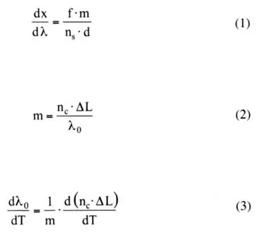
Once the chip attach materials are defined, the grating must be controlled to a constant temperature to maintain center wavelength characteristics. The relationship between center wavelength and temperature is described by the dispersion of the focal position x with respect to wavelength () (Equation 1) and the diffraction order of the grating (m) (Equation 2). Equation 3 states that the change in the center wavelength increases in proportion to the temperature dependence of the optical path length [1]. If typical material coefficients are entered into the equations, the calculated variation in center wavelength is on the order of 10 pm/oC.
 |
|
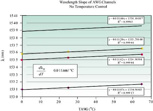
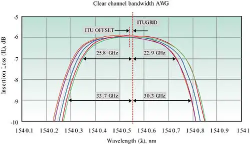
Figure 2 shows measured center wavelength drift characteristics of a typical AWG indicating a slope of ~11pm/oC. Figure 3 shows a typical single channel measurement of center wavelength drift over temperature for a controlled waveguide. The clear channel bandwidth is affected for that and every channel on the chip. Without temperature control, the AWG would only be usable in a narrow band of ambient temperatures. To maintain reasonable center wavelength control the temperature is controlled to better than �0.5oC and for best performance better than �0.1oC over the ambient temperature range of -5oC to +70oC.
 |
Figure 2. Measured center wavelength drift.
 |
Figure 3. Temperature effect on clear channel bandwidth.
Temperature distribution at the grating and across the arrayed waveguides is also critical requiring detailed thermal analysis of the silicon chip, its mounting materials and configuration, the package and the environment.
PLC temperature control schemes can be of heat-only or heat-cool designs depending on the temperature required for optimum performance. The lowest cost and highest reliability method is to utilize process parameters that set the operating temperature above the specified maximum ambient temperature utilizing a heat-only approach. This design simplifies the electrical circuitry requirements and increases the reliability of the component by avoiding the use of thermoelectric coolers (TEC). To achieve accurate temperature control the system must be evaluated for several variables. These variables include sensor type and placement, control element selection and positioning, and a suitable temperature control system.
Sensor Selection
Size, cost, accuracy, and long term stability need to be considered. Popular sensors for these applications are either platinum resistance thermometer devices (RTD) or transition metal oxide thermistors. Thermocouples are not recommended due to accuracy, aging characteristics, non-linear response and sensitive electronics required for proper implementation. Semiconductor diodes can also be used but for highest accuracy each junction must be calibrated individually. Platinum RTD elements are recognized internationally as a standard for temperature measurement. This class of sensors typically have positive temperature coefficients (PTC) and have relatively linear response over the temperature range of 0 to 100oC. Accuracy and repeatability of RTD elements is excellent with errors of 0.1% or less. Stability over time is also outstanding for RTD elements due to the nature of the materials used in the construction.
Thermistor elements are also resistive temperature devices. The most accurate and versatile elements have negative temperature coefficients (NTC) but have non-linear response to temperature. This makes the element harder to use over a wide range of temperatures, but for specific temperature ranges the accuracy can be calibrated to less than 1%. Stability over time is not as good as platinum RTD elements, but is very good with a 10 year drift delta of ~1%. Packaging for thermistors varies and is selected based on the position and mounting style for the application.
Sensor Location
Proximity of the sensor to the controlled element is key to minimize thermal resistances between them. As the ambient temperature changes, the power required to maintain a given grating temperature will also change. Because the grating is sensitive to stress, sensors and heating elements cannot be placed in direct contact using high modulus materials. Low modulus, high thermal conductivity materials may be used but attaching sensors directly to the grating is avoided. The temperature difference between the sensor and the grating is expressed in Equation 4.
|
Control Element Selection
If a heat-only solution is acceptable the heater selection must take into account the area that needs to be controlled and how and where to apply the element, the form-factor and space allowances in the package, and the electrical characteristics of the end-user power supplies. Because PLC die are relatively large (typical 60 x 40mm) and the temperature gradients must be minimized across this area, selection of the heater elements is narrowed somewhat. Foil backed polyimide strip heaters are popular due to the ease of application and wide range of standard sizes and resistances. Resistive heaters embedded into substrate are also used as a temperature control element as well as a mechanical mount for the chip.
For heat-cool applications, TECs are used. TEC (or Peltier) devices enable temperature control at any temperature within the capability of the chosen element. In heat mode, a TEC will operate much like a resistive heater, but in the cooling mode efficiency drops off dramatically making the control quite inefficient. Modern TECs have a wide operating temperature range and can withstand high levels of shock and vibration. Reliability concerns for TECs focus on high humidity environments that can affect the aging properties of the couples that make up the component.
For heat-only and heat-cool designs, the electrical characteristics should be selected to provide a reasonable value that can be used with a single voltage supply. Typical voltage supplies for telecom applications are 12, 5 and 3.3V supplying 1 to 5A for each device.
Control Element Placement
Placement of the control element must consider the shape and size of the controlled area. Maximizing thermal coupling between the element and the grating is essential while providing the most compact geometry and minimized heat loss to the environment. Small variations in the placement of the element can cause changes in the performance of the device so assembly procedures must be carefully specified. Electrical connections should not interfere with the temperature distribution of the chip, nor should they be placed where they may be damaged or worked loose from shock or vibration. Thermal modeling of the heater placement may be necessary to minimize the center wavelength drift over temperature.
Temperature Controllers
Typical temperature controllers for AWG components are closed-loop controls with feedback from the sensors and proportional power output to the control element. Linear and pulse-width modulation (PWM) controller designs are utilized with proportional temperature control to allow fast ramp and very stable temperature control over varied ambient conditions.
Linear temperature controllers are usually simple analog designs. Set points and control parameters are usually set with manual potentiometers or resistance selection and no digital communications are provided. Linear controllers require heat sinks because the output transistors generate high levels of heat during high load conditions. These designs are usually low noise and very accurate but voltage drop across the output transistors limits the load resistance to a narrow range depending on the supply voltage and current.
PWM controllers offer an alternative to linear circuit designs. Because the output transistors are biased full on or full off most of the time, very little heat is generated in these components and heat sinks are generally not required. This makes the design very compact and more versatile. PWM controllers typically use a microcontroller and allow digital communications with the host computer.
One drawback of PWM designs is power supply noise. Because the transistors are biased from full on to full off very quickly, transient noise spikes can wreak havoc on power supply systems that have other devices on the same bus. Careful selection of PWM frequency is necessary for filter design and to minimize the size of filtering components such as inductors and capacitors.
Conclusion
It can be easily seen that planar waveguide packaging is a daunting challenge, but the problems can be solved using an array of tools. Thermal, mechanical, materials, process, assembly, and electrical engineering are necessary for successful implementation of these components into a robust, high performance product. More research and development is being conducted on integrated PLC devices and new and innovative techniques must be developed to enable low-cost, high-yield products. Hybrid techniques are being investigated for assembly of active components to integrated PLC devices, thereby creating a complete solution for optical networking in a single package. Nanotechnology and MEMS technology are also being integrated into PLC devices for highly sophisticated systems. As these integrated solutions are developed and refined the impact on high bandwidth for communications networks will be dramatic, enabling lower cost and greater level of service for the end user.
References
- Ishii, M., Hibino,Y., Hanawa, F., Nakagome, H., and Kato, K., “Packaging and Environmental Stability of Thermally Controlled Arrayed-Waveguide Grating Multiplexer Module with Thermoelectric Device”, Journal of Lightwave Technology, Vol. 16, No. 2, February, 1988.
- Ehlers, H., Biletzke, M., Kuhlow, B., Przyrembel, G., and Fischer, U.H.P., “Optoelectronic Packaging of Arrayed-Waveguide Grating Modules and Their Environmental Stability Tests”, Optical Fiber Technology, No 6, pp 344-356, 2000.
- Tarter, T. and McKeen, J., “Thermal Management Challenges of Integrated Planar Waveguide Devices”, Second Annual IEEE Photonic Devices and Systems Packaging Symposium, July 2002.
- Cohn, M., Roehnelt, R., Xu, J.H., Shteinberg, A. and Cheung, S., “Integration and Packaging of MEMS”, Second Annual IEEE Photonic Devices and Systems Packaging Symposium, July 2002.


