Introduction
While emerging methodologies correctly insist that thermal engineers should be involved right from the early conceptual stages of electronics product design [1], many situations still require thermal analysis well after the introduction of the product to its intended application. Military transmitters installed in the 1980’s and 1990’s and still in operation today are an example. Due to increased reliability requirements and the prohibitively high cost to replace or upgrade existing electrical designs, the thermal conditions within these transmitters are now of greater interest.
|
||||||
An application using forced air cooling of an RF signal amplifier (see Figure 1) has been studied. The main heat dissipating components on the printed circuit board (PCB) are mounted directly to an extruded aluminum heat sink situated in airflows of approximately 100 l/sec. The amplifier provides up to 440 W of output power and contains four high power output transistors (Philips BLW96) each dissipating 130 W to the heat sink through a package footprint of 1.96 cm2 [2]. Due to the remote location of the transmitter sites, amplifiers operate in ambient air temperatures of up to 50°C with the pre-heated cooling air at the inlet to some heat sinks reaching 60°C.
A comprehensive program was developed to determine the thermal conditions within 440 W amplifiers and to evaluate methods for reducing the junction temperature of the output transistors. Experimental techniques and numerical simulations were used to study the various thermal paths from the transistor junction to the cooling airflow. This article presents the detailed results of the following areas of investigation:
- Laboratory and field tests to determine transistor temperatures in operational amplifiers.
- Experimental evaluation of various thermal interface materials.
Field Measurements
A thermal map of the PCB at maximum power, taken using an infrared camera (see Figure 2), shows the highly localized nature of the heat sources (i.e., the output transistors and the bank of resistors directly below them). However, due to the varying surface emissivities, reliable absolute component temperatures cannot be obtained from this initial image. As a result, laboratory experiments employing a simplified DC circuit to power individual transistors were used to obtain a better estimate of junction temperatures in the field. A subsequent infrared image, taken with the PCB removed and the top surfaces of the heat sink and transistors painted black to provide a constant known emissivity, showed a transistor case temperature of 83°C at maximum transistor power dissipation. Using thermocouple measurements of the transistor flange and inlet air temperatures the transistor case temperature of 83°C was shown to correspond to a junction temperature of approximately 160°C at 20°C ambient. By heating the inlet air, it was estimated that junction temperatures reached the manufacturer’s maximum rated level of 200°C [3] when inlet air temperature reached 60.9°C.
 |
Figure 2. Infrared image of transistors and resistors on circuit board at full output power.To test these predictions, an amplifier was instrumented for temperature measurements at the transmitter site. A single, K-type thermocouple was attached to a mounting screw on each of the output transistors while a thermocouple mounted at the heat sink inlet measured air temperature. Assuming an essentially one dimensional heat transfer path, the transistor junction temperatures were calculated as follows:
Tjunct = Tsc + (Rth fl-sc + Rth junct-fl) Q (1)
|
||||||||||||||||||
Thermal resistance from the junction to the mounting screw is split into two components. Rth junct-fl is defined by the transistor manufacturer [3] and Rth fl-sc was determined in earlier laboratory experiments where Tsc and flange temperature, Tfl, were monitored for a range of Q. Since field experiments were conducted on a live transmitter network, it was not possible to insert thermocouples inside the transistor flange. Hence the screw temperature had to be used to estimate flange temperature and, subsequently, junction temperature. However for all laboratory experiments a thermocouple embedded in a 0.9 mm diameter hole drilled halfway through the flange of each transistor (see Figure 1b) allowed direct measurement of Tfl (i.e. let Rth fl-sc = 0 in equation 1).In the field, 26 separate tests were conducted in order to determine the transistor junction temperature at various ambient air temperatures between 21.5 and 34.7°C. For comparison purposes, the average maximum transistor junction temperature from each test was then extrapolated to reflect ambient conditions of 60.9°C. The results showed a significant variation in maximum junction temperatures due to fluctuations in key electrical parameters in the field (i.e., changing signal frequency effects transistor efficiency and fluctuations in power reflection from the antenna back to the amplifiers effect transistor workload). However, the maximum junction temperatures recorded in the field compared favorably with laboratory estimates and confirmed that under 60°C ambient air conditions it is possible for transistor junction temperatures to exceed the maximum rated temperature of 200°C.
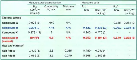
Table 1. Thermal Resistance of Interface Materials Selected for Trials
|
|||||||||||
Thermal Interface Materials
Table 1 lists various thermal interface material (TIM) candidates along with selected published data. The label “Compound D” refers to the thermal grease that is currently applied at the transistor/ heat sink interface to fill the air gaps that exist due to surface non-flatness and roughness. It has a relatively low specified thermal conductivity of 0.6 W/m�K [4] (i.e., much higher than 0.026 W/m�K for air but much lower than 150 W/m�K for the heat sink).
 |
Figure 3. Schematic of experimental setup (side view).One of the problems with using published thermal data for TIMs is that the test apparatus used to obtain these results are largely idealized and often don’t adequately resemble the intended application. Various researchers have investigated the thermal resistance across contact surfaces and identified the need to test TIMs under typical field conditions (i.e., application specific values of contact pressure, surface flatness, and surface roughness) [5-8]. As such, experiments have been conducted to allow a back-to-back comparison of selected commercial interface materials in this application and to quantify the difference between published and application specific thermal resistance data. Figure 3 shows part of the experimental configuration used in this study. Here thermal resistance is defined as:
 |
|
Gap pad A and Gap pad B are thermal pad materials with published thermal conductivities well above that of the current grease. The drawback with thermal pads is the finite minimum thickness over which the heat must pass and their inability to flow in and fill the microscopic surface roughness interstices. Compound A and Compound B are thermal greases, which were selected as having relatively high published values of thermal conductivity while Compound C provided a mid-range value.
Two separate sets of experiments were conducted with TIMs applied:
- Per the standard field assembly procedure.
- After careful preparation of the interface surfaces.
Standard Field Assembly
Initial trials involved all TIMs except for Compound A. Between tests the transistor and heat sink surfaces were cleaned with isopropanol to remove any existing heat sink compound residue. No extra surface preparation was carried out. Thermal grease compounds were applied thinly to both the flange and pedestal surfaces and the excess removed using a straight edge. The mounting screws were tightened to between 1.25 and 1.35 Nm. A nominal airflow of 100 l/s was imposed over the heat sink, and flange and pedestal temperatures were recorded. Flange temperatures were used to calculate transistor junction temperatures using equation 1 (with Rth fl-sc=0) and Rth int was calculated using
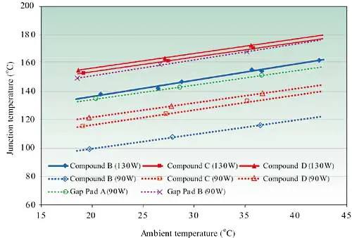
Figure 4 plots transistor junction temperature versus ambient air temperature for 90 W (dotted lines) and 130 W (full lines) dissipation per transistor. The thermal pad materials performed poorly in this application, with junction temperatures rising by almost 27°C against the Compound D at 90 W °C was noted when comparing Compound B to the current grease, at 130 W dissipation.
 |
Figure 4. Comparison of transistor junction temperatures for various TIMs at 130W and 90W dissipation levels.
Careful Surface Preparation
Further trials were conducted using Compounds A, B, and D to address the specific issues of surface cleanliness, roughness, and flatness. The contact surfaces were cleaned with emery paper placed over a known flat surface between each test. This not only removed previous TIM contamination but also ensured consistent flatness and roughness of the flange and pedestal surfaces. Prior inspection of 20 failed transistors showed that surface flatness is a major variable in this application with just over 50% of the transistors exhibiting a gap in excess of 0.025 mm between the middle of the flange (i.e., the area directly below the junction) and a known flat surface. This was attributed to warping of the
The final column of Table 1 shows reduced values of Rth int for both Compound B and Compound D after careful contact surface preparation. In the case of Compound D the interface resistance fell 40% from 0.494Kcm2/W to 0.292Kcm2/W. This represents a drop in device temperature of 13.4°C at 2/W representing a further drop of 7.6°C.
In this application Compound A performed marginally better than the current Compound D. However, the results for Compound A were somewhat disappointing when compared to the published data and illustrate the importance of obtaining application specific data for use in detailed design of thermal paths in electronics cooling.
Conclusion
While temperature drop across the interface between high power electronic components and heat sinks contributes significantly to the component temperature, significant reductions are possible through careful selection of the thermal interface material and preparation of contacting surfaces to reduce thermal resistance. Experiments conducted here produced a similar performance ranking of selected TIMs to that obtained using published data (except for Compound A, which dropped one position in testing here). However, measured values of thermal resistance differed from published values by up to 37%, highlighting the importance of obtaining accurate, application specific thermal
References
- Belady, C.L. and Minichiello, A., “Effective Thermal Design for Electronic Systems”, Electronics Cooling, Vol. 9, No. 2, pp. 16-21, 2003.
- Maguire, L., Behnia, M., and Morrison, G., “An Experimental and Computational Study of Heat Transfer in High Power Amplifiers”, Journal of Heat Transfer Engineering, (in Press), 2003.
- Phillips Semiconductors, “Data Sheet: BLW96 HF/VHF Power Transistor”, pp. 1-14, 1986.
- Dow Corning, “Product Information: Dow Corning 340 Heat Sink Compound”, pp. 1-2, 2000.
- Gwinn, J.P. and Webb, R.L., “Performance and Testing of Thermal Interface Materials”, Microelectronics Journal, Vol. 34, No. 3, pp. 215-222, 2003.
- Getkin, V., Ankireddi, S., Jones, J., Pecavar, S., and Hundt, P., “Characterizing Bulk Thermal Conductivity and Interface Contact Resistance of Thermal Interface Materials in Electronic Cooling Applications”, Proceedings IPACK03 International Electronic Packaging Technical Conference and Exhibition, Maui, HI, Paper no. IPACK2003-35324, 2003.
- Blazej, D., “Thermal Interface Materials”, Electronics Cooling, Vol. 9, No. 4, pp. 14-20, 2003.
- Lasance, C.J.M., “Problems with Thermal Interface Material Measurements: Suggestions for Improvement”, Electronics Cooling, Vol. 9, No. 4, pp. 22-29, 2003.


