Introduction
Heat transfer in and around a printed circuit board (PCB) is generally very complex. Some of the heat generated in components is conducted away through the multiple conducting (trace) layers, vias, and dielectric layers of the board; and some is dissipated by convection and radiation from the exposed surfaces. There has long been a focus on characterizing the cooling airflow, with many papers written on the subject and much physical testing performed. Computational fluid dynamics (CFD) software that can accurately predict the cooling airflow over typical PCBs is commercially available. It is common practice to compute the temperature distribution within the board and its components by coupling a simplistic heat conduction model for the PCB together with these CFD models.
In this simplistic model, the details of the conduction paths within the PCB are smeared out into a single homogeneous layer that represents the entire PCB in an averaged or effective manner. Obviously, there are inhomogeneous details such as vias concentrated under a component or traces conducting heat directly away from a component that cannot be captured accurately with this approach. Nevertheless, this method has been widely used because it is readily available in commercial software systems. Recently, though, a new approach has become available [1], employing a more accurate and detailed representation of the PCB heat conduction processes using a new finite element analysis (FEA) based modeling procedure. This article briefly describes the new approach.
Specification of Trace Layers and Vias
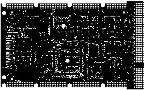
The starting point here is the output file from an electrical CAD (ECAD) program used for electrical design of a board. This file specifies the geometry and material properties of the traces on each layer and the vias. ECAD files typically contain two types of detailed mathematical descriptions for traces. The first type describes the trace outline using a closed polygon that is filled by trace material. It is referred to here as a “filled trace”. A complex but not uncommon example is shown in Figure 1. The second type describes the centerline of a constant width trace using a set of straight-line segments. It is referred to here as a “line trace”. Figure 2 shows an example PCB having both types of traces in a layer, with the filled traces shown as solid red.
 |
Figure 1. A power plane defined by a single closed polygon having over 80,000 points.Vias are holes that are drilled in the board and then plated with copper to make electrical connections between traces that are on different layers of the board. Vias can be “thru” vias where they go completely through the board, “blind” vias where they enter one side and stop at an internal layer, and “buried” vias where they connect between internal layers of the board. Thermally, vias play a significant roll in locally enhancing the heat conduction through the board thickness because the thermal conductivity of copper can be as much as 1200 times that of common dielectric materials.
Finite Element Representation of Trace and Dielectric Layers
In FEA the objects to be modeled are divided into many smaller pieces, called “elements,” within which the complex heat transfer processes are approximated by simpler algebraic equations involving the temperatures at a finite number of points called “nodes” [2]. The list of available element types includes three-dimensional (3D) “solid” elements, such as hexahedrons (bricks), tetrahedrons, and wedges; two-dimensional (2D) “plate” elements, such as triangles and quadrilaterals; and one-dimensional “resistor” elements.
The simplest approach to modeling heat conduction within a PCB would be to create an extremely fine mesh of solid elements that incorporates every detail in three-dimensions, no matter how small. This approach is considered completely unfeasible because the model size would be prohibitively large for typical PCBs. Today’s multi-layer boards can have as many as 50 layers and thousands of complex traces.
The finite element model described here makes use of realistic approximations to incorporate the important heat conduction details, yet keep the model size feasible for rapid solution on the latest generation of PCs. First, the thermal conductivity of the copper trace layers is high enough that the temperature gradient through these thin layers can be neglected. This allows a two-dimensional mesh of elements to represent the in-plane heat conduction for a typical trace layer containing thin line traces and/or larger solid copper areas. In the present application, an unstructured triangular mesh is used to accommodate the complex geometrical features of the PCB and the outlines of the attached components, enabling accurate modeling of the PCB boundary conditions and the component connections. Each dielectric layer in the PCB is modeled by a single layer of wedge-shaped solid elements, enabling heat conduction between the copper (trace) layers to be modeled accurately. An efficient and automatic mesh generation procedure based upon extruding an initial 2D mesh of triangles is employed here to obtain the layers of nodes and elements.
In order to keep the model size reasonable, the triangular mesh does not explicitly represent the polygonal boundaries of the individual traces. Instead, each triangular plate region is given effective anisotropic conductivity properties, computed to represent the line traces and solid copper regions within its boundary. The finite element model is actually created by converting these plate elements directly into a triangular network of resistor elements, each given its own unique and appropriate resistance. This is much simpler than creating many thousands of plate elements, each having unique anisotropic material properties, and the thermal conductivity of these traces is still accurately accounted for. With a reasonably fine initial 2D mesh of triangles, the complex temperature distributions in the PCB are well represented, and the component temperatures are computed accurately. For complex boards with many layers and hundreds of traces, it is not unusual to obtain 2D meshes containing 5,000 or more triangles.
Computation of the resistor network representing a filled trace is done as follows. First, for each triangle that is completely within the trace boundary, the triangle is converted into three thermal resistors that exactly represent the thermal conductivity of the corresponding solid copper triangular plate. For triangles that are only partially inside the trace boundary, the three resistors are computed as above, but the resistance values are then adjusted (increased) to account for the reduced conducting area, and resistors are omitted where the conduction path is interrupted.
Computation of the resistor network representing a line trace is done as follows. The centerline of the trace is described by a set of straight-line segments, each of which overlaps one or more triangles along its path. For each overlap, the portion of the straight-line segment that overlaps is converted into a thermal conductor, which is then transformed into a set of three equivalent thermal resistors aligned with the triangle edges and connected to nodes at the corners.
Automatic construction of the initial 2D mesh of triangles is performed in a three-step procedure. First, an appropriate set of straight-line segments representing the boundaries of important geometrical details is created. Second, the geometry is cleaned up by removing segment intersections and by organizing the straight-line boundary segments into closed loops and regions. Finally, a set of nicely shaped triangles (with no small interior angles) is created using a numerical procedure named deLaunay mesh generation [3], which is well known in the computational geometry literature.
The 3D finite element PCB model is obtained from the initial 2D triangle mesh through the following “extrusion” process. First, the nodes in the 2D triangle mesh are copied onto many planes at the appropriate positions through the PCB thickness. These nodes are then connected to the wedge-shaped solid elements representing the dielectric layers. Next, the planar resistor networks representing the conducting layers are connected to these nodes. Finally, the resistors representing vias are added. In the typical situation where conducting layers alternate with dielectric layers, each plane of nodes connects to resistors representing a conducting layer, plus the solid elements representing dielectric layers above and/or below the conducting layer.
 |
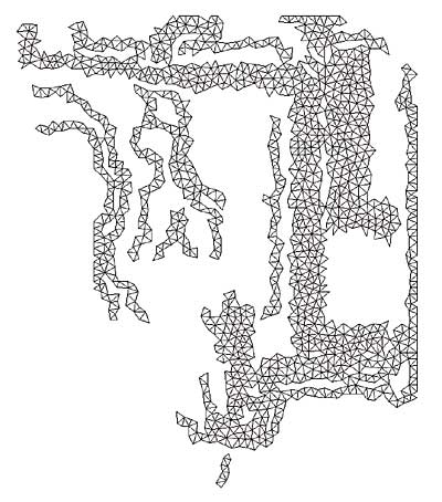
Figure 2. Typical conducting layer with filled and line traces.Figures 2 and 3 illustrate a typical conducting layer with many filled and unfilled traces and its finite element equivalent resistor network. Note that many traces can overlap an individual triangle. Clearly, many more elements would be necessary to represent the interior of each line trace explicitly by plate elements, and each trace outline would have to be constructed based upon the line width and centerline.
 |
Figure 3. Equivalent resistor network for the typical conducting layer shown in Figure 2.
Representation of Vias
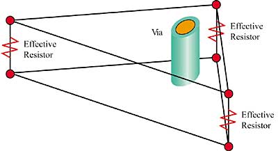
Thermal vias connecting trace layers are modeled by adding effective resistor elements connecting between the corresponding layers of nodes in the copper trace layers. Similar to the methodology used in representing individual traces, resistor elements are added at the specific meshed element where the via resides to enhance the local heat transfer through the board. This is illustrated in Figure 4. The three resistance values account for the properties and geometry of the via and the location of the via within the element. The resistors are only connected to the layers to which the via is electrically connected.
 |
Figure 4. Representation of an individual via using effective resistors.
Example
Figure 5 shows the results of a simple example calculation where heat is applied uniformly to three rectangular regions of a board in which conduction within the traces plays an important role. The board has a pair of conducting layers like the one shown in Figure 2, sandwiched around a dielectric layer, and the board is cooled by convection from the top and bottom surfaces. The temperature contours in Figure 5 clearly indicate patterns of higher temperatures where heat is conducted along the traces. These local details are missed using the effective board approach.
 |
Figure 5. Simple heat conduction example.
Conclusions
This article has described an efficient procedure for accurately modeling the conduction of heat within the layers of a printed circuit board using finite element analysis. This procedure is based upon separate representations of the dielectric and conducting layers. A key feature is the use of an equivalent resistor network to represent the traces in a conducting layer and vias between layers. In this manner, the size of the finite element model is kept manageable, while key details are preserved for an accurate solution.
References
- TASPCB software, from Harvard Thermal, Inc.
- Hughes, T.J.R, The Finite Element Method, Prentice Hall International Editions, 1987.
- O’Rourke, J., Computational Geometry in C, Cambridge Univ. Press, 2000.


