Introduction
Despite the slowdown in the communication industry, Internet traffic continues to grow rapidly, fueled by the explosion in data communications, mobile Internet, e-commerce, content rich applications, and multi-media services. Internet traffic has increased by approximately 80% yearly in each of the last three years, and will continue to grow at 60 – 80% annually through year 2006 [1]. At the same time, network power requirements will scale with capacity growth. Keeping in mind that traffic demands will soon reach tens of Tbps, power demands may limit or decelerate network growth.
This article describes an important network aspect from a power density perspective: How many Watts (W) are required to transfer, switch, or process a bit of information per second? More importantly, the article deals with arising challenges in that field, particularly if the network growth continues at the current pace. Overall, the article intends to address the majority of the following questions:
- How do we respond to the growing power demands in communication networks? With the reduced bandwidth predictions, is the problem still as severe as it was predicted in 1999 and 2000, during the higher growth period?
- What are the unique cooling management issues in telecom applications versus other industrial applications? What is the biggest problem area in network equipment design: node, shelf, board, or device (chip) level? What trends in terms of W/cm2 are seen in these applications? What key electronics technologies would be required to cope successfully with the problem? What cooling technologies might be required?
- How long can existing technologies be used to address the problems in thermal management for telecom applications? When will a revolutionary new technology or technologies be required?
To provide the relevant analysis, both current and future point of presence (PoP) power efficiencies are assessed. Results from that analysis indicate that network power is expected to reach unprecedented limits, posting numerous challenges for research, design community and applications. Furthermore, the breakdown of network power distribution is evaluated, helping to locate the most critical network functionalities. Finally, the solution space is searched within a novel network architecture based on an all-optical network and feasible equipment design.
To address the topic, a few terms are frequently used. To properly understand them, these definitions are provided:
- Power Efficiency (W/Gbps) – Equipment, system, or network overall power dissipation (W) required to transfer, switch, route, or process a Gigabit of information per second (Gbps).
- Traditional (Current) Communication Networks – Networks where signals are transferred between electrical and optical domains frequently due to the need for their transmission, switching, routing, conversion, or amplification.
- All-Optical Network (AON) – Predominantly optical transport network with a limited number of conversions back into the electrical domain; usually referred to as a “next generation network”.
- Point of Presence (PoP) and Central Office (CO) – Physical place where communication equipment is located. CO is more related to telephone equipment while PoP involves both data and phone communication equipment.
- Internet Protocol (IP), Time-Division Multiplexing (TDM), Asynchronous Transfer Mode (ATM) – Different standards or technologies to transfer signals through the network.
- Regeneration – Process during which an optical signal is transferred into the electrical domain, amplified, and transferred back to the optical domain.
PoP Power Efficiency (W/Gbps) and Power Projections
According to NEMI roadmaps [3,4], telecommunication equipment located in PoPs and COs leads industrial applications in terms of dissipated power. The majority of today’s network power is consumed by providing the functionality for transport, switching, routing, processing, regeneration, and storage. The goal of this section is to analyze the power efficiency of large traffic nodes currently in operation (PoPs or COs), and to assess if any concern regarding power dissipation could occur in the future. Therefore, if necessary, up-front, timely development might eliminate any issues in years to come.
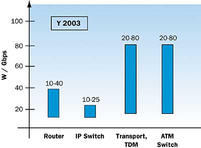
The current high traffic nodes contain equipment for optical transport, data core, interconnect, add/drop and edge aggregation. Today’s market suppliers of communication equipment strive in providing efficient equipment. An analysis of power efficiency of current telecommunication equipment suppliers [2] has given the following results: a) routers (10 – 40 W/Gbps), b) IP multi-protocol switches (10 – 25 W/Gbps), c) transport / TDM equipment (20 – 80 W/Gbps), and d) ATM switches (20 – 80 W/Gbps), as shown in Figure 1. Based on the power efficiency to transfer Gbps in the network and equipment that may be located in PoPs and COs, it is expected that an efficient PoP or CO might have the power efficiency of 50 W/Gbps. Assuming 2 Tbps traffic in large nodes today, a dissipation of around 100 kW is predicted. Consequently, the PoP or CO operators who manage today’s high traffic PoPs or COs are expressing their concerns, particularly for the situation when they have to add new equipment. Power dissipated poses additional concerns, along with cost implications (space, air conditioning, etc.).
 |
Figure 1. Power efficiency of telecommunication equipment [2].By assuming the traffic growth as stated by telecom analysts (RHK or Corning [1]), the bandwidth demand will continue to grow at 60 – 80% annually through year 2006. Even with the assumption that the power reduction per function will continue to follow Moore’s Law (improvement doubles every 18 months), we might expect to reach over 300 kW at large PoPs and COs in 2006! Over the next couple of years, power consumption will continue to grow between 5 to 15% yearly, where the higher percentage refers to device and module levels, and the lower percentage to shelf and system levels [2,3,4].
Another aspect needs to be mentioned. The signal data rate will continue to grow due to network capacity growth. For every quadrupling of the rate (e.g., from 2.5 Gbps to 10 Gbps, or tomorrow from 10 Gbps to 40 Gbps), power dissipation increases 2 – 2.5 times. Based on physical limits of currently dominant air forced convection technologies, it appears that some disruptive technologies and design solutions might soon be required.
Overall, the network traffic growth poses challenges at every level such as:
- Building power provisioning and heat removal of several hundreds of kW (node level)
- Cost optimization of energy, air-conditioning, and real estate (node level)
- Temperature control for reliable operation to prevent failure (shelf level)
- Heat removal by direct liquid or immersion cooling (shelf and board level)
- Need for cost effective unconventional cooling solutions (shelf level)
- Low effective thermal resistance and low pressure, high-conductivity interfaces (board level)
- Thermal integration with electromagnetic compatibility (EMC) for high speed, low voltage circuits (board level)
- Efficient heat spreading, thermal interface materials (board level)
- Heat removal from high flux chips (device level)
- Higher thermal conductive packaging materials, such as spreaders, adhesives, and thermal pastes (device and board level)
- Precise temperature control and low operating temperature (device level)
- Need for higher reliability and efficiency of thermo-electric cooling (device level).
In response to the projected network power, particularly in PoPs or COs, it is the right time for the industry to create a new design and architecture space to address the power-density challenges of next generation networks [5,6]. There are two aspects for the response to the above challenges: network architecture based on an all-optical network (AON), and feasible telecommunications equipment design.
Solution Space – Network Architecture and Feasible Equipment Design
Current communication networks exercise various functionalities to transfer a bit of information from one user to another: transmission, switching, processing, routing, or storage. The goal is to find out the power distribution in the network, identify the most critical functionalities from a dissipation viewpoint, and propose an industry response.
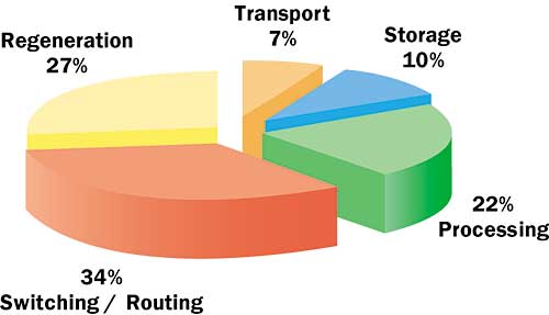
With inevitable generalization and assumptions, the power distribution in the network is expressed in Figure 2. It is noticeable that just three functionalities strongly participate in power usage, having the following distribution: processing (22%), switching/routing (34%), and electrical regeneration (27%). Based on the previous section analysis, current communication networks require 50 to 100 W to transfer a Gbps, having an efficiency within the 50 – 100 W/Gbps range.
 |
Figure 2. Network power distribution [7].Therefore, minimizing the total power per network throughput is the main architectural goal, focusing on the three most contributing functionalities. The achievement of this goal heavily depends on the ability to transfer the bits in the optical domain with minimal transfer to the electrical domain. The ability to keep a signal in the optical domain, as it travels from the point that it enters a network, until the point that it leaves, brings a clear benefit from the power density standpoint. The so-called all-optical network (AON) is going to be an enabler in developing a “less power hungry” network, with the added benefit of being able to cope successfully with the expected network growth and cost reduction requirements.
It is important to mention that electrical packet-level switching, storage, and processing will continue to place increasing power demands for the foreseeable future. However, the deployment of optically-based devices, such as optical amplifiers, tunable lasers, parallel optical interconnects [9], wavelength converters, adaptive optics, etc., as well as network architectures based on all-optical technologies, will be able to bring significant benefits in the range of a fivefold improvement. The analysis shows that the power efficiency for such a network would be within the 10 – 20 W/Gbps range [7].
The second aspect deals with feasible telecommunications equipment design. The key is in exploring techniques and technologies for reducing power at the source. Integrating industry state of the art advances in high-density packaging, high speed interconnects and materials will bring the results. PCB technologies such as micro-via, embedded passives, and low thermal impedance substrates are the basis for very high speed Cu PCB interconnects. When combined with parallel VCSEL-based opto-electronics, SiGe, InP, GaAs, and deep sub-micron CMOS technology, industry leading shelf capacity results [10].
At the same time, thermal management technologies continue to evolve rapidly due to the market requirements for high chip heat fluxes, densely populated boards, multi-kW shelves, and high-density frames. More stringent cost, performance, and reliability constraints make thermal management one of the key enabling technologies in the development of telecommunications equipment for next generation networks.
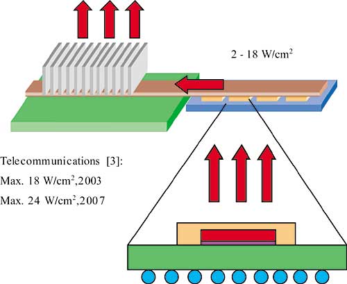
Conventional thermal techniques, based on forced air cooling, are very close to their performance limits. New techniques, including such cooling technologies as micro/macro heat pipes (Figure 3) and liquid cooling, will have to be developed and implemented. On the other hand, cooling of opto-electronics systems requires precise temperature control and low operating temperatures. By successfully overcoming these challenges, thermal management will contribute to the increased competitiveness of packaged telecommunications products. Further advances and development are projected in the following thermal management areas: thermal spreaders, heat pipes, water cooling, refrigeration cooling, thermal interfaces, thermoelectric cooling, and direct immersion cooling.
 |
Figure 3. Enhanced thermal solution for high thermal dissipation [7,8].
Conclusions
Network power requirements will continue to increase with Internet capacity growth. Power dissipation in large PoPs or COs will soon reach a couple of hundred kW. There are two aspects for the response to that challenge: architecture based on an all-optical network, and feasible telecommunications equipment design.
Maximizing the use of optical technologies in all-optical network architectures will ultimately deliver the lowest power per function for transport, amplification, and wavelength switching in tomorrow’s networks. However, electrical packet-level switching, storage, and processing will continue to place increasing power demands for the foreseeable future.
Feasible equipment design is expected to focus around the development of reduction in power at source-per-function and enhanced thermal management. Although there are no short-term disruptive technologies on the horizon, the industry needs to complement dense PCB technologies, low power CMOS, high speed copper, and optical interconnects with key improvements in new materials (SiGe, InP, GaAs, etc.) and advanced thermal concepts that show both reduced power and cost.
References
- Lightwave Online, “Corning Estimates Fibre Market”, March 26, 2003.
- Vukovic, A., “Comparative Analysis of Power Efficiency of Telecommunication Equipment from Different Vendors”, Communications Research Centre proprietary documentation, May 2003.
- NEMI Technology Roadmap, Edition 2000.
- NEMI Technology Roadmap, Edition 2002.
- Vukovic, A., “Power Density Challenges of Next Generation Telecommunication Networks”, ElectronicsCooling, Volume 9, Number 1, February 2003.
- Vukovic, A., Watkins, J., Vukovic, M., “Power Density Challenges of Next Generation IP Networks”, WTC / ISS2000 Conference, Birmingham, UK, 2000.
- Vukovic, A., “All-Optical Networks – Impact of Power Density”, Panel on “Challenges of Electronic and Optical Packaging in Telecom and Datacom Equipment”, Maui, Hawaii, USA, July 2003.
- The National Technology Roadmaps for Semiconductors, Semiconductor Industry Association, 1997.
- Zenz, A., Gregory, B., “Parallel Optical Interconnects Take Hold in Networks”, Integrated Communications Design, July 2002.
- Suhir, E., “The Future of Microelectronics and Photonics and the Role of Mechanics and Materials”, IEEE/CPMT Electronics Packaging Technology Conference, 1997.


