Introduction
Small Form Factor (SFF) optical transceiver packages for use at 1-2 Gbits/s data rates have been described by several authors [1-5]. These rely on dual miniature optical connectors such as the MT-RJ or the LC to provide optical-component case widths as small as one centimeter. Passive alignment of the optical fibers with the active optical devices is achieved with the assistance of a Silicon Optical Bench (SiOB) containing V-grooves used for self-alignment of fibers and/or a guide ferrule to the SiOB bearing the active optical devices [1-4]. This article examines options to achieve a similar package size with optical devices intended for high-power optical applications at much higher data rates implemented in a Ball Grid Array (BGA) package format that integrates the optics and electronics data handling functions.
This article illustrates a paper-study to determine how such goals might be achieved. The initial results of an analysis on aspects of the assembly and in-service reliability of such a package structure is presented. The critical remaining design and manufacturing technologies that must be addressed to finalize such a design are also identified. For the most part, the details of the design approach examined are not optical-device specific, within the bounds set by power losses, alignment requirements, and temperature stability requirements. But for the most compact designs, the LC connector option and TO packaging option for the active optical devices is precluded. In the following, we discuss how specific design goals define the package design rules. The resulting assembly options for the optical package architecture are also considered as are our findings regarding aspects of the module reliability and the likely functionality of the design and its possible variants.
Generic Module Layout
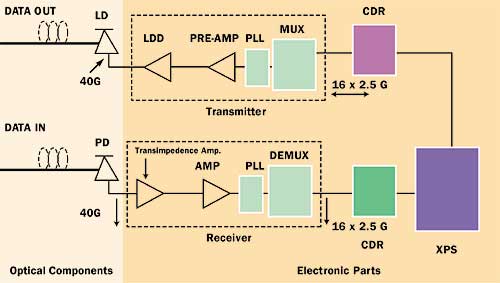
One variant of the proposed opto-electronics transceiver module structure is illustrated in Figure 1. All of the electronic sub-systems are mounted on a BGA substrate separate from an enclosed case containing just the optical components.
 |
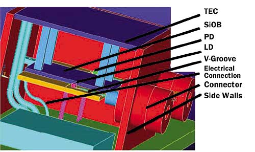
Figure 1. Generic layout for the proposed opto-electronics module package.The separate optical canister, shown in Figure 2, may be either mounted to or built as an integral part of a BGA package carrying the multiplexer (MUX) and de-multiplexer (DMUX) assemblies and the laser diode (LD) driver and the DMUX preamplifier. The intention is to use readily available lower-cost laser diodes. Consequently, the optical components will be cooled with a thermoelectric cooler (TEC). With one design variant, for use with 125-micron core fibers, the proposed design automatically provides the highest possible coupling factor between input/output fibers and Physical Media Dependent (PMD) devices. This will eliminate the need for a costly pre-alignment process step, lowering the manufacturing cost substantially.
 |
Figure 2. Cutaway view of the inside of the optical canister.From a manufacturing point of view, the proposed design and its variants can provide a convenient separate assembly path for the entire optical component portion of the module. Or, just the fiber-related portion of the module can be added to the rest of the package as one of the final assembly steps. Specific care in the design has been taken to provide optimized thermal distribution paths for both the optical and electronic components to prevent self-background heating within the module and to meet thermal stability requirements.
Design Objectives
- The optical sub-unit would integrate receiving and transmitting functions up to 40 GHz in its various versions.
- The optical sub-unit could employ 10-micron fiber technology.
- An inexpensive LD, requiring thermoelectric cooling, would be utilized.
- The package would contain integrated MUX and DMUX capabilities on a common substrate with a separate, sealed package holding two optical components (a photodiode [PD] in addition to the LD).
- A Ball Grid Array packaging platform would be utilized.
- Standard or at least easily available miniature optical fiber connectors would be employed.
- The entire package footprint would be less than 20 x 30 x 15 mm, with the optical transceiver section itself no larger than 10 x 10 mm, not including the extensions of the optical fiber connectors away from the optical subunit’s side wall.
Design Optimization Methodology
The seven design goals impose certain logical constraints on the over-all design configuration and assembly options.
Thermal Management
TECs are notoriously inefficient as heat pumps. They may almost triple the total heat energy that must be sunk to hold the LD and PD at a desired temperature for a typical 1.5 – 2 Watt thermal load generated by the two devices in tandem. For a conventional butterfly package design, the strategy is to sink the TEC to the package substrate, which, in turn, can be bonded to a metal heat sink. Electrical connections are then made through the top of the package (through long butterfly-lead wings) so that a minimum of the exhausted heat is returned through the leads to the package. In a BGA design the TEC exhaust heat cannot be removed to the BGA substrate. If it were, a substantial amount of heat would re-circulate back into the package itself. This imposes two limitations on our design:
Design Rule 1: The LD and PD must be cooled with a top-mounted heat sink.
Design Rule 2: The TEC must be mounted to the top of the optical subpackage with the thermal output of the TEC connected inside to the top of the optical canister. This inverted design is also optimal in terms of the impact of connective heat transfer external to the package.
Optical Fiber-LD Alignment
Various self-aligning schemes using optical benches are practical for 125-micron fiber-based systems. But these lack the accuracy needed for alignment of 10-micron core single mode fibers essential to high data rate applications. A variety of special “in package” alignment schemes have also been described, based upon MEMs options [6], which could accomplish this step at a lower cost. But it is unclear when these products will be readily available for such an application. The 10-micron fiber requirement rules out passive self-alignment options for the top-level design of package. The state of the art in assembly of optical transceivers using 10-micron fibers is that a final active alignment of the LD beam to the fiber must be made. Adjustment sensitivity well less than 1.0 micron is required to optimize the power coupling. In general, this is accomplished by using a computer controlled station to manipulate an individual fiber to achieve a maximum power output from an operating LD; then by attaching the fiber and ferule assembly to the optical package once the sweet-spot has been located.
The additional constraint of our design-size goal makes this option untenable. The need for inserting the mechanical manipulator tool inside the package to grip the fiber to make the alignment raises the likely package width above the desired size limit. This situation leads to the following design requirements:
Design Rule 3: The optical connector for the transmitter must be mounted to the optical package sidewall before the final LD-to-fiber micro-alignment is made.
Design Rule 4: The final mechanical alignment of the fiber to the LD will be done by manipulating a portion of the optical package itself. This means that a final assembly step will, in all likelihood, involve jointing two sections of the optical package together.
Mechanical Reliability Considerations
Several microns of movement of an optical fiber connector mounted to the optical subpackage can be anticipated with ambient temperature changes. An unacceptable tilting of the fiber axis may also occur. Counter balancing these movements, by somehow matching the CTE’s of the internal-LD-support structures with the canister sidewall, is not an option. The temperature of most of those internal structures will be staked to the cold-side temperature of the TEC. Micron offsets cannot be tolerated with 10-micron fiber technology. There is only one design option. In the final assembly, the LD and the free end of the optical fiber and the ferrule guiding assembly extending into the package from the sidewall connector must be mechanically joined in close proximity on a common secondary substrate, such as a SiOB.
Clearly the LD will be pre-mounted to the bench and the remainder of the attachments will be accomplished as an integral part of the final assembly. To minimize demands upon the TEC (and hence upon its size), the laser driver along with the MUX, DMUX, and DMUX preamplifier will be placed on the BGA substrate. Substantial wasted heat from these assemblies cannot be allowed to reach the active optical devices. The LD and PD must be suspended in some fashion above the substrate, but still electrically connected to it and mechanically stable. It seems that these connections cannot readily be made unless they are established prior to the final assembly of the optical canister.
Design Rule 4 requires that the section of the optical canister containing the fiber connector be brought into the final assembly from the top while the optical bench, upon which the LD sits, is oriented with the LD on top of the bench to allow final optical package assembly. Yet from Design Rule 2, the bench must also attach from its topside to the inverted TEC. This leaves us with the following design requirements.
Design Rule 5: The laser driver, MUX, DMUX, and DMUX preamplifier must be mounted on the BGA substrate.
Design Rule 6: PD and LDs must be placed upon one or more secondary structures (SiOB) suspended (at least before final assembly) above a lower substrate (either the BGA substrate itself or a separate optical canister bottom substrate) by their electrical connections.
Design Rule 7: The active PD and LD devices must be positioned on the topside of the SiOB.
Design Rule 8: The LD and PD will be placed on the opposite wings of a secondary substrate, with a free area in between to make an attachment to the inverted TEC’s cooling top plate. For reasons discussed later, it may be preferable to use a composite secondary structure to meet this rule, containing a SiOB as a subcomponent.
Design Rule 9: The optical I/O attachment to the optical bench will be made as one of the final assembly steps.
The LD-fiber alignment is by far the most critical. Any position solution that satisfies the requirements of good coupling to the LD will, with a good ferrule package design, automatically satisfy the requirement for acceptable fiber alignment with the PD.
Optical Package Design and Assembly Procedures
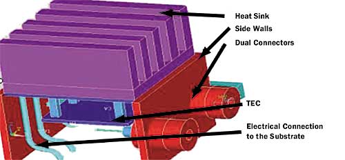
The package shown fully assembled in Figure 1 meets all of these design constraints. There are several assembly options to achieve the desired optical-canister architecture. For all of these, one of the subassemblies will consist of the top section of an optical canister with four substructures, which is shown in Figure 3. These are a top-mounted convective heat-sink, a five-sided canister for the optical components, an internally mounted TEC with the power supply leads extending through the opened sixth side, and a pre-mounted connector for the incoming and outgoing optical fibers. The latter would be mounted on a common canister sidewall with fibers and a guide ferrule of appropriate dimensions to reach the optical bench within the unit.
 |
Figure 3. Top section of the optical canister prior to final assembly.The bottom section of the optical package will, prior to final assembly, contain three elements: A SiOB containing V-grooves for coarse alignment and a pre-mounted PD and LD devices; vias through the silicon to bring the power and signal connections to the two active optical units; and leads of an appropriate length running from the bench to a substrate.
The substrate, which forms the bottom of the optical canister, may either be the BGA substrate itself or an independent substrate to build a standalone optical package. The optical fibers may have either a 125-micron or a 10-micron core. If the 10-micron option is selected, then a computer-controlled alignment step will be required during final assembly. If not, the V-grooves in the bench could provide the required alignments, such as described by Iwase [1] et al. Sufficient space between the optical bench and the optical canister walls must be allowed. There are two issues: The TEC power leads will be attached to the substrate first; then the canister will be rotated to slip the top of the canister into an approximately correct position. There must be sufficient space to allow this maneuver. A cursory analysis indicates that a 2-mm internal clearance should be more than adequate.
Module Fabrication and Reliability Analysis
The optical fibers themselves can tolerate substantial bending without suffering damage. The small differential displacements that the two ends of both sets of fibers (i.e., PD input and LD output) will likely experience during assembly will easily be an order of magnitude higher than they will encounter during service as a result of the differential-thermal-expansion-induced displacements between their optical connectors and their optical bench ends. The properties of the epoxy used to stake the optical structure to the bench will need to be adjusted to insure that the forces generated during the alignment procedure, in the presence of the coupling epoxy, are not excessive.
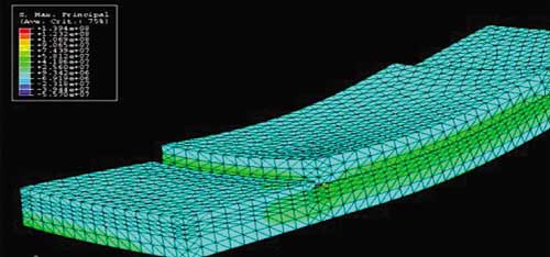
Differential expansion between the silicon optical bench and the TEC will be kept to a minimum during service. After all, the purpose of the TEC is to stabilize the temperature of the active optical devices as well as to cool them. Although the top surface material of most TECs is BeO, optimum for an interface with the cooler’s diodes, the predicted cyclic thermal strains in the interface epoxy of the TEC and a silicon bench is not seen as an issue in joint reliability for the design. A finite element analysis [9] of the strains in the epoxy and of the peak stresses in the silicon for both assembly and service conditions shows both to be deep in the safe zone. The predicted peak stress in the silicon, shown in Figure 4, barely approaches 20% of its expected fracture strength.
 |
Figure 4. Thermal-contraction-induced tensile stress in the silicon optical bench resulting from cooling to room temperature from 200°C.
Summary
Design aspects of a proposed opto-electronic transceiver module have been studied to meet the needs for a package with flexible fabrication options for the commercial LAN market. Low cost and small package size in a BGA format are the main drivers for the design discussed. Such needs translate into feature and performance design objectives, which have been defined in this article. In turn these objectives place constraints upon the most critical aspect of the design: a stand-alone optical-transceiver package, thermoelectrically cooled and containing just the LD and PD active devices.
Several design rules have been identified for this submodule, which speak to the way the optical package must be assembled in addition to the overall package structure. The resulting design is discussed along with an analysis of various aspects of its likely reliability. Three key issues in the further development of the proposed module have been noted: 1) a ferrule/fiber/SiOB interface design; 2) an optimal transmission-line lead design for connection of the SiOB to the BGA substrate; and 3) appropriate design measures to deal with transmitter-receiver crosstalk.
References
- Iwase, M., Nomura, T., Izawa, A., Mori, H., Tamura, S., Shirai, T., and Kamiya, T., “Single Mode Fiber MT-RJ SFF Transceiver Module Using Optical Subassembly with a New Shielded Silicon Optical Bench,” IEEE Transactions on Advanced Packaging, Vol. 24, No. 4, November 2001.
- Abe, S., Tobita, K., Shinozaki, T., Arai, K., Takeshita, K., Tanaka, K., and Isono, Y., “Short Wave SFF Small Form Factor Transceivers,” 51st Electronic Components and Technology Conference Proceedings, pp. 30-34, 2001.
- Owen, M., “Agilent Technologies’ Singlemode Small Form Factor (SFF) Module Incorporates Micromachined Silicon Automated Passive Alignment, and Non-Hermetic Packaging to Enable the Next Generation of Low-Cost Fiber Optic Transceivers,” IEEE Transactions on Advanced Packaging, Vol. 23, No. 2, May 2000.
- Sunaga, Y., Takahashi, R., Tokoro, T., and Kobayashi, M., “2 Gbit/s Small Form Factor Fiber-Optic Transceiver for Single Mode Optical Fiber,” IEEE Transactions on Advanced Packaging, Vol. 23, No. 2, May 2000.
- Hogan, W. K., and Giao, D. P., “A Novel Low-Cost Small-Form-Factor Transceiver Module,” 50th Electronic Components and Technology Conference Proceedings, pp. 725-732, 2000.
- US Patent Numbers 5,606,635; 5,602,955; and 5,553,182.
- Matick, R. E., Transmission Lines for Digital and Communication Networks, The McGraw Hill Book Company, 1969.
- Johnson, W.C., Transmission Lines and Networks, The McGraw Hill Book Company, 1950.
- Hibbitt, Karlsson & Sorenson, Inc., http://www.abaqus.com


