Introduction
In the 1990’s, with the advent of surface mounting of semiconductor packages, multilayer printed circuit boards and multilayer substrates for Ball Grid Array packages were introduced. In order to create electrical interconnections between the different metal layers, vias are fabricated [1]. In most cases vias are hollow cylinders of copper, created by plating a thin layer on the inside surface of a hole drilled through the laminated metal and dielectric layers. As was soon discovered, vias not only provided an electrical path through the dielectric layers but also an enhanced thermal path for heat flow.
This column will examine a simple example involving heat generated on the surface of a silicon chip and flowing through a dielectric substrate with varying numbers of vias. It will evaluate two different analytical methods of calculating the thermal resistance of this “stack up.”
Finite Element Analysis Thermal Solution
Figure 1 depicts the situation of interest: A die is adhesively bonded to a laminate consisting of a BT substrate sandwiched between two copper layers. The two metal layers are electrically connected together by a matrix of vias.
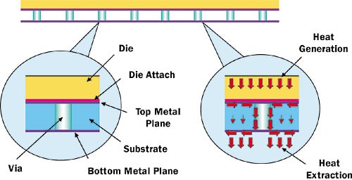 |
Figure 1. Diagram of silicon die attached to two-layer substrate with via array.Figure 1 also illustrates the heat flow between the top surface of the die and the underside of the lower copper plane for a small region centered about one of the vias. The heat is generated uniformly on the surface of the die. The heat is intercepted by the top metal plane. Because of the high thermal conductivity of the copper compared to that of the BT, most of the heat will converge to the via location, flow along the length of the via, and then diverge upon reaching the bottom metal plane. A small portion of the heat will flow directly from the top plane to the bottom one through the substrate.
The heat is then removed from the bottom metal layer with a thermal efficiency that would be representative of an array of solder balls covering 20% of the surface of the bottom layer. This is represented in the model as an effective heat transfer coefficient applied to the bottom surface.
The solution was generated using a commercial finite element analysis program, in which the features of interest were generated with a high level of fidelity. For example, the vias were represented as hollow cylinders using extruded 16-sided polygons [2]. Because of the level of detail and the dense finite element mesh employed, the results of the FEA solution are considered to be “exact.”
The detailed geometrical and material property assumptions are listed in Table 1. The die is assumed to be a square, 10 mm on a side. All of the other planar components are assumed to have the same width. Hence, the area A is the same for all components. The copper layers are 35 �m thick (commonly referred to as “one-ounce” copper). The dimensions and materials are chosen to be ones commonly found in BGA packages.
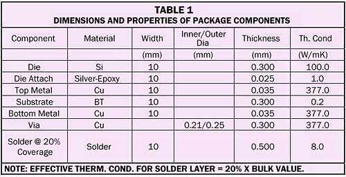 |
Table 2 lists the various via configurations included in the analysis. All of the via arrays are assumed to be on a regular pitch on a grid pattern. The via matrices vary from no vias (0 x 0) to a large 11 x 11 array. The thermal resistance for the zero via situation is 15.9°C/W. This thermal resistance is reduced by 90% at the largest via array evaluated.
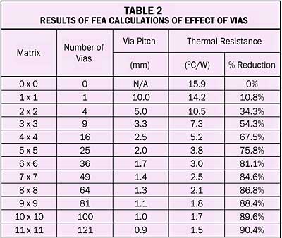 |
Figure 2a graphically depicts the relationship between the calculated thermal resistance and the number of vias. After a certain point, adding additional vias becomes a matter of diminishing returns. For example, a 6 x 6 matrix of thermal vias achieves 90% of the thermal reduction obtained with the 11 x 11 array.
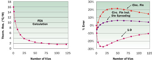 |
Figure 2a. FEA thermal solution.
Figure 2b. % error of various analytical methods. (+ error indicates value larger than FEA solution).
Analytical Methods
We will explore two analytical methods. The first is the thermal engineer’s first line of defense: the 1-dimensional (1-D) heat flow model. The second is based on a calculation explored in a previous column: the circular fin.
1-Dimensional Model
The mechanics of 1-D heat flow analyses have been explored in this column previously [3, 4]. The required equations for performing this calculation are presented in Table 3. Equation 1 represents total thermal resistance of the entire structure. The term with the summation accounts for the thermal resistances of all the layers with the exception of the substrate. The second term accounts for the resistance network of the substrate including the vias.
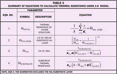 |
We must keep in mind that the 1-D model is based on the assumption that all of the heat flux lines are parallel. Hence, it would not account for the additional thermal resistance due to the converging and diverging heat flows in the top and bottom metal layers.
Figure 2b contains a graph showing the percentage error in the 1-D solution compared with the FEA solution. The error exceeds 10% except for the case with zero vias and is as high as 27% for 9 through 16 vias. Worse, the calculation underestimates the thermal resistance.
Circular Fin Model
Another approach to the calculation is to adopt the circular fin model [5] to account for the converging and diverging heat flow the top and bottom planes. The first step is to define a unit cell, centered about a particular via. Figure 3 illustrates this concept. The width of the top and bottom plates are each equal to the via pitch. The heat transfer from the top of the die to the top plane and the bottom plane to the bottom of the solder layer are represented by heat transfer coefficients, hEFF, TOP and hEFF, BOT, whose magnitude is calculated from the thickness and conductivity of the material layers bounding each metal layer. The heat spreading ability of each plane is represented by the product of the thermal conductivity and thickness of each plane, kEFF x tEFF.
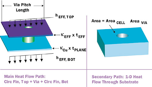 |
Figure 3. Application of circular fin model to unit cell of via array.The secondary heat flow through the block of substrate in the unit cell may be represented with adequate accuracy assuming 1-D heat flow.
Table IV provides the equations required to perform the calculations. Equation 5 provides the solution of the thermal network, assuming the two parallel paths within each cell as illustrated in Figure 3. The total resistance is equal to the resistance for a unit cell divided by the total number of vias.
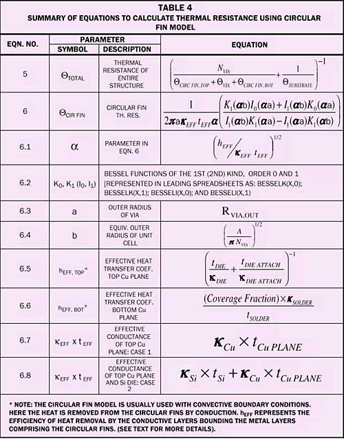 |
The supplementary equations to calculate the values of the individual thermal resistances are provided in the remainder of Table 4 and Equations 3 and 4 in Table 3. Of note is Equation 6, which calculates the thermal resistance of a circular fin. This equation contains terms involving Bessel functions. Although they are rarely encountered outside of math classes these days, they are found in all the leading spreadsheets and have the form indicated in item 6.2 of Table 4.
Figure 2b graphs the error associated with the use of the circular fin approach with two different assumptions for the conductance of the top fin, as explained below.
Case 1: Standard Circular Fin Calculation
The first assumes, quite naturally, that the appropriate values for the conductivity and thickness for the top circular fin are simply equal to the thermal conductivity of the top metal plane times its thickness, as indicated in Equation 6.7. This curve is labeled “Circ. Fin” in the graph. The maximum error associated with this approach is 22%. This is an improvement over the 1-D model and, since these values exceed the exact ones, it represents a conservative calculation.
Case 2: Circular Fin Calculation Including Heat Spreading by the Die
The second assumption is derived from the observation that the conductance ( x t) of the Si die is actually greater than that of the top copper plane. Hence the die will also contribute to the heat spreading. Equation 6.5 is used to calculation the appropriate value of kEFF x tEFF to account for the combined heat spreading ability of the die and the top metal plane. The results of this calculation are represented by the remaining curve in the graph. In this case, the maximum error is only 6% and, as with the previous calculation is a conservative value. This represents a significant improvement of the other two methods.
Conclusions
Thermal vias can be a very effective design feature for reducing the through-thickness thermal resistance of multilayer substrates.
The use of the circular fin equation to account for the spreading of heat in the laminate metal layers leads to greater accuracy than that obtained with 1-D calculations, which ignore these effects. The spreading effect due to the silicon die itself should be taken to account for further improvement of the accuracy of the calculation.
References
- Guenin, B., “The Many Flavors of BGA Packages,” ElectronicsCooling, Vol. 8, No.1, 2002, pp. 32-40.
- ANSYS, Version 8.0.
- Guenin, B., “One-Dimensional Heat Flow,” ElectronicsCooling, Vol. 3, No.3, 1997, p. 15.
- Guenin, B., “Conduction Heat Transfer in a Printed Circuit Board,” ElectronicsCooling, Vol. 4, No.2, 1998, p. 13.
- Guenin, B., “Convection and Radiation Heat Loss from a Printed Circuit Board,” Electronics Cooling, Vol. 4, No.3, 1998, p. 13.


