Introduction
Since their introduction, multilayer printed circuit boards have provided a significant benefit to the thermal management of IC packages. As is widely recognized, the power and ground planes in these boards function as fins and spread the heat beyond the package footprint and enhance heat transfer to the air. Heat can flow into these planes by conduction either through thermal vias or through the dielectric layers of the board. In either case, there is an excess temperature difference associated with heat flow from the surface of the board to the internal planes.
Quite frequently, when heat transfer from a package to a board is analyzed, the board is treated as a homogeneous solid with values of effective thermal conductivity calculated from volume-weighted averages of the conductivity of the constituent materials [1]. These calculations neglect what are here referred to as “entrance effects” in analogy to excess pressure drops that occur in fluid flow at the entrance of channels. Not including these entrance effects can lead to a significant underestimate of the thermal resistance for heat to flow from the contact region with the package to the planes of the board. These entrance effects can be calculated only by accounting for the details of heat flow into the small-scale metal structures of the PCB, namely the vias and surface traces.
This column will explore heat transfer from surface traces on a multi-layer PCB to the interior planes. It will begin with a detailed Finite Element Analysis (FEA) of the PCB to elucidate the physics of the heat flow and to generate a series of “exact” solution to the problem. It will then explore the use of analytical expressions which can be used to calculate the thermal resistance of the board, accounting for the “entrance effects” with reasonable accuracy.
Finite Element Analysis
As has been discussed in an earlier column, for an IC package attached to a PCB, there are two distinct regions in the board in terms of heat transfer mechanisms: 1) the region within the package footprint (the outline of the package and its leads as viewed from above) and 2) the region beyond the package footprint [2]. This analysis will deal with only with heat transfer in region 2.
For convenience, the assumed board construction will correspond, in general to that of a JEDEC-standard high-conductivity test board [3]. The model will deviate from the dictates of the standard by varying the width and thickness of the traces to explore their effect on heat transfer to the planes.
The board consists of six layers: the top metal traces, two interior planes, and three dielectric layers. Since the analysis deals only with region 2 of the board, the portion of the board that would normally be located under the package footprint is missing.
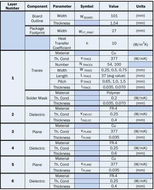
Table 1 lists the details of the package construction and of the parameters used to represent the package in the two modeling approaches. In the case of parameters employed in the analytical models, the symbols used to represent them in the relevant equations are provided.
Table 1. Values of Inputs to FEA and Analytical Models.
A number of thermal simulations were performed using a commercial FEA code, varying the trace width, pitch, and thickness as indicated in Table 1 [4]. Identical heat loads were applied to the cross-section of each trace exposed by the cutout at the package footprint. This approach essentially “pumps” heat into each trace as if it had been routed to the trace from a package lead (located, of course, within the package footprint). The total power, P, is simply equal to the individual heat load times the number of leads. A convective boundary condition was applied at the top and bottom surfaces of the board. Both the heat transfer coefficient, h, and the ambient air temperature, TAIR, are assumed to be constant. For the results presented here, a single value of h was used, namely 10 W/m2K. This is typical of a natural convection cooling environment.
In a few cases, the heat was injected directly into the planes at the cutout surface. This was intended to provide benchmark solutions in which there would be no entrance effects.
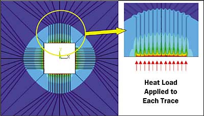
Figure 1 serves to illustrate both the board construction and details of the thermal solution. Figure 1a depicts temperature contours for the top of the board. A predominately radial heat flow is observed. The inset illustrates the temperature contours near the region of heat injection. Figure 1b shows the temperature contours along a cut through the centerline of the board. It clearly indicates a region of high thermal gradient near the inner edge of the board. With increasing distance from this edge, the temperature along the board thickness becomes much more uniform.
Figure 1a
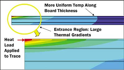 |
Figure 1bFigure 1a. Temperature contour maps showing top surface of board.
1b. Temperature contour map along cut through centerline.The board-to-air thermal resistance was calculated in the usual way,
 |
where the maximum board temperature, TBOARD,MAX was measured at the inner edge of the board.
Figures 2a and 2b provide graphs of BOARD-AIR versus trace width for all values of trace number, pitch, and thickness investigated. Increasing any of these parameters except for the pitch increases the actual amount of copper in the traces and leads to a reduction in
BOARD-AIR by increasing the conductance of the trace layer.
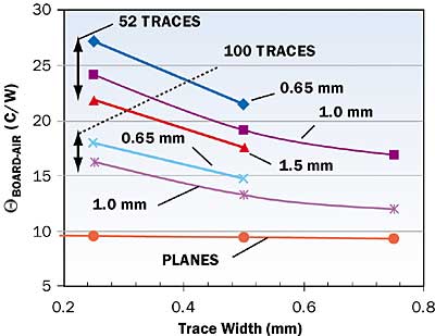 |
Figure 2a
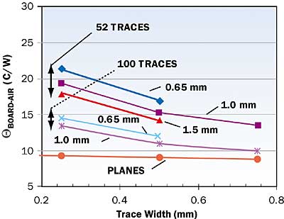 |
Figure 2bFigure 2. Results of FEA calculations. In 2a, trace thickness is 0.035 mm;
in 2b, trace thickness is 0.07 mm. The values 0.65, 1.0, and 1.5 mm indicate the trace pitch.If each of the trace parameters save for the pitch is held constant, then increasing the pitch also leads to a reduction in BOARD-AIR. This is due not to any change in the trace conductance, but to the heat spreading mechanism within the upper plane itself. An increased pitch for the same number of traces will cause the heat to be injected into a larger area of the board, reducing the need for additional heat spreading by the plane and diminishing the associated temperature rise in the plane.Also indicated are values of
BOARD-AIR calculated by applying the heat load directly to the inner edge of the planes. These represent a lower bound for
BOARD-AIR. The difference between a point on one of the upper curves and that on the lower curve represents the magnitude of the thermal entrance effect for a board of a particular trace design. The thermal entrance effects vary from a minimum of 1°C to a maximum of 18°C.
Analytical Calculations
An inspection of the temperature contours in Figure 1 suggests that each of the traces may be considered to be a fin that injects heat into the upper plane as the remaining heat flows along the trace length. Once the heat has been injected into the planes, it is well established that the resultant heat flow along the planes and into the air can be described using a circular fin model.
Calculation Method
The calculation method to be explored here is as follows:
- Calculate the thermal resistance for heat to flow from an individual trace to the upper plane,
TRACE-PLANE, using a linear fin model. The total resistance for heat to flow from all the traces into the board is equal to
TRACE-PLANE/NTRACES.
- Calculate thermal resistance for the heat to flow from the planes to air,
PLANE-AIR, using a circular fin approximation.
- Calculate the board-to-air from the following expression:
 |
The following sections provide details for each step of the calculation and compare the accuracy of its predictions with those of the FEA approach.
Linear Fin Model
Heat transfer from a finite linear fin to air has been discussed in a previous column [5]. This same formulism will be used in the present article, with the exception that heat will be transmitted across a constant thickness of dielectric to the board plane rather than into the air by means of convection. The concept is exactly the same. One can view the ratio of DIELEC/tDIELEC as an effective heat transfer coefficient. (A similar use of a circular fin model in a purely conductive heat transfer situation was discussed in this column in the previous issue [6].)The sequence of equations needed to calculate
TRACE-PLANE is provided in Table 2. Equations 3.1 – 3.2 are the usual ones for applying the linear fin model.Table 2. Summary of equations to calculate the trace-to-plane thermal resistance using a linear fin model
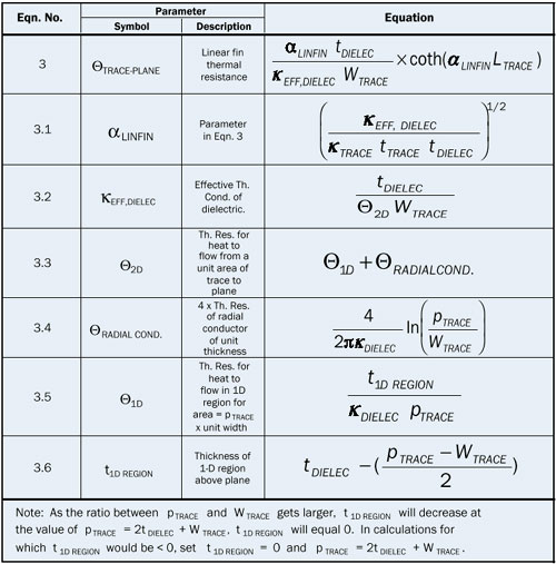 |
Equations 3.3 – 3.6 are used to account for the fact that, since the trace pitch is greater than the trace width, the heat will diverge as it flows from the trace to the plane.
These equations represent the diverging part of the flow by a radial conductor and the remaining part as a 1D heat flow element. The end result of applying these equations is a calculated value of an effective thermal conductivity, EFF-DIELEC, applied to the dielectric separating the trace from the plane. Where there is a diverging flow,
EFF-DIELEC, will be greater than
DIELEC.The advantage of accounting for the diverging flow using
EFF-DIELEC is that it allows Equation 3.1 to have the same form is it does for a 1D flow situation. The accuracy of Equations 3.3 – 3.6 has been confirmed by this author to agree with 2D FEA simulations to within 10% for a trace pitch to width ratio up to 3 to 1
Circular Fin Model
The use of a circular fin to calculate the thermal resistance for the portion of a board beyond a package has been described in a previous column [5]. The sequence of equations to calculate PLANE-AIR is presented in Table 3. In this calculation, only the conductivity of the copper planes is taken into account. The thermal role of the dielectrics can be neglected in the plane-to-air thermal calculations. All of the equations in Table 3 are standard, with one exception: Equation 4.2. This equation calculates an effective thickness for the copper plane in the model that not only includes the full thickness of the two planes, but also a term representing an area averaged trace layer thickness, determined at a specific radius from the board center.Table 3. Summary of equations to calculate the plane-to-air thermal resistance using a circular fin model
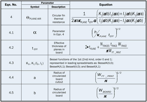 |
Equation 3.2 calculates this smeared layer thickness for the traces at an arbitrary value of radius equal to WFT-PRNT/2.
Calculated Results
Figures 3a and 3b compare the results generated using the above equations with the FEA results. The error ranges from -1 to 26%. In general, the error is less than 10% for traces for which the pitch-to-width ratio is less than 2. The falloff in accuracy for ratios greater than 2 is apparently due to limitations of the simple model represented by Equations 3.3 to 3.6, used to calculate the effect of the diverging heat flow on the local heat transfer between the trace and the plane.
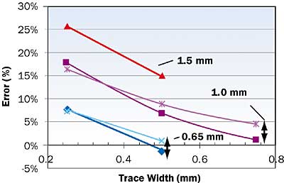 |
Figure 3a
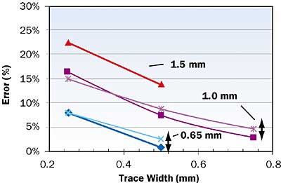 |
Figure 3bFigure 3. Comparison of results of analytical with FEA calculations. In 3a, trace thickness is 0.035 mm; in 3b, trace thickness is 0.07 mm. The values 0.65, 1.0, and 1.5 mm indicate the trace pitch. (+ Error indicates value larger than FEA solution.)
Conclusions
Entrance effects in the flow of heat from the surface of a multilayer PCB into its inner planes can account for a significant temperature rise. Those striving for accuracy in either FEA or analytical models must account for the details of heat flow into the small-scale metal structures of the PCB.
References
- Guenin, B., “Conduction Heat Transfer in a Printed Circuit Board”, ElectronicsCooling,” Vol. 4, No.2, 1998.
- Guenin, B., “Convection and Radiation Heat Loss from a Printed Circuit Board”, ElectronicsCooling”, Vol. 4, No.3, 1998.
- See, for example: JEDEC Standard JESD51- 7, “High Effective Thermal Conductivity Test Board for Leaded Surface Mount Packages,” available for free download at www.jedec.org.
- ANSYS, Version 8.0.
- Guenin, B. “Convection and Radiation Loss from a Fin”, ElectronicsCooling, Vol. 5, No. 1, 1999.
- Guenin, B., “Thermal Vias – A Packaging Engineer’s Best Friend”, ElectronicsCooling,” Vol. 10, No. 3, 2004.

