Introduction
The growing pressure to fit as much circuitry into the smallest space possible has created new and more acute thermal problems for the design engineer. More high power components in a smaller space means higher watt densities, which lead to increased heat. As the operating temperatures of components within a design increase, their performance, stability, and life expectancy decrease, thus compromising the usefulness of the overall product design.
Insulated metal circuits (IMCs) provide heatsinking and heatspreading to keep components running cool, and therefore allow designers to implement high power density designs that deliver the kind of functionality demanded by customers in many market sectors.
Adopting IMCs can also greatly simplify designs. By converting an existing power board design from a through-hole FR4 layout with leaded transistors, heatsinks, transistor clips, fixing screws, and interface pads to a surface mount IMC equivalent, the weight, size, and component count can all be significantly reduced. In certain scenarios IMC can obviate the need for the heatsinks and other hardware. There is also a potential saving in assembly time that may prove important in high volume or cost sensitive products.
Insulated metal printed circuits use the same basic design rules as conventional FR4 circuit layouts. They have familiar rules applying to details such as the shape and size of land patterns and component spacing, meaning that the designer need not acquire new skills. The inherent robustness of IMCs with their metal baseplates makes the job of designing with the material much easier.
Applications for IMCs come from many sectors of the electronics industry. When the material first became available approximately ten years ago, most applications were in products such as drive controls and DC/DC converters. As designers packed more functionality into smaller spaces, applications arose in different areas of a product’s electronic design. The rapid growth in portable electronics brought new applications. Besides being compact, portable equipment often needs to be housed in rugged, durable, sealed enclosures. This makes the inclusion of ventilation features to assist heat transfer by convection impossible due to the risk of moisture and dust ingress.
IMC Construction
In its simplest form the material consists of a metal base plate and a copper foil circuitry layer bonded together with a thin thermally conductive, electrically isolating adhesive. In unprocessed form, the material is available in sheets ranging in size from 305 x 457 mm to 457 x 609 mm. The size of the panel selected by the customer largely depends on the length and width of their particular circuit board design and how efficiently it can be stepped and repeated around the master IMC panel to give minimum wastage.
A range of baseplate materials and thicknesses are available. Aluminum is the most popular because of its excellent thermal conductivity, light weight, and relatively low cost. Another option is copper, which although more expensive than aluminum, has excellent thermal performance and is compatible with existing printed circuit chemistry. The final and most expensive options are copper – molybdenum – copper (Cu-Mo-Cu) or copper – invar – copper (CIC).
Available baseplate thicknesses are typically 1.0, 1.6, and 2.0 mm. For some applications the baseplate itself can perform the role of heatsink. In others where there is a greater watt density and hence more power to dissipate, the baseplate only acts as a heatspreader (Figure 1) and needs to be attached to a larger heatsink or the chassis of the product itself to achieve acceptable levels of heat dissipation.
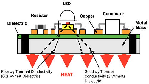 |
Figure 1. A high degree of heat spreading and dissipation resulting in a lower component temperature when using IMC.
The thermally efficient dielectric layer is the key to IMCs. It performs three major functions: heat conduction, electrical insulation, and a method of bonding the circuit layer to the baseplate. Without it, the concept of metal-based circuits would not exist.
The thickness of the dielectric layer ranges from 75 to 300 microns. At 100 microns the material delivers a thermal resistance in the region of 0.035 K/W for a T0220 device. Quoted bulk value thermal conductivity is approximately 3 W/mK in X, Y and Z planes; important for heat spreading. A dielectric strength of 800 V per each 25 microns of dielectric layer thickness is typically achieved. If increased isolation and capacitance between the baseplate and copper circuitry layer are required, then the dielectric material can be applied in thicker layers.
Compared with dielectric materials used to insulate metals in other thermally efficient printed circuit board approaches, such as alumina, the boron nitride thermal filler used in IMCs is less abrasive, allowing it to be easily drilled, punched, and formed. This is critical when producing the final PCB profile and detail, such as mechanical fixing points. The dielectrics used in IMCs have a high degree of flexibility (Figure 2), allowing the material to be formed into right angles and even fully formed tubular parts, which would be impossible with both FR4 and high performance materials, such as direct bond copper (DBC) ceramic substrates. This gives the potential to use IMC as a thermally efficient circuit board and chassis in one.
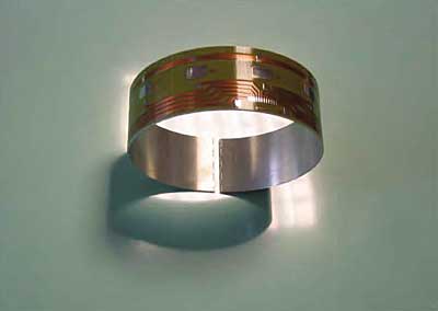 |
Figure 2. The mechanical characteristics of the dielectric allow parts manufactured using IMC to be formed into tight curves without compromising performance.
IMC laminate can be produced using copper circuitry thicknesses ranging from 17 to 420 microns. The selection criteria for choosing copper thickness for a specific application is based on the same considerations as is the case for a conventional FR4 circuit; primarily current carrying requirements. Typically a high ductility, electrodeposited copper is used.
Going Multilayer
In addition to basic single-sided boards, it is also possible to achieve multilayer constructions that allow greater circuit density by utilizing inner layers (Figure 3). A double-sided laminate (DSL) that has a dielectric with 3 W/mK thermal conductivity separating two layers of copper, gives approximately ten times the thermal conductivity of a comparable thickness of FR4 (0.3 W/mK). This simple sandwich construction can be printed and etched with plated through vias just like a regular double-sided FR4 circuit. DSL assemblies can be used alone or incorporated into a metal-based board. By combining processed DSL assemblies separated and bonded together with further dielectric layers, finished IMCs with any number of layers can be fabricated. Plated vias, blind and buried vias, and mounting holes are all possible, giving a very high degree of design flexibility.
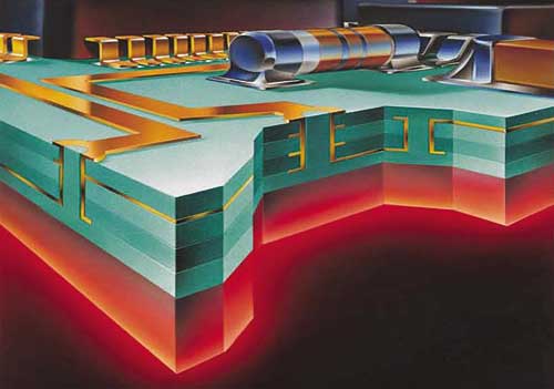 |
Figure 3. A multilayer construction using IMC.
Processing
As previously mentioned IMCs are processed in much the same way as FR4. The only significant difference is that the metal base plate needs to be protected from the etchant used to create the finished copper tracks and lands by a polyester film, which can be peeled away after processing.
The straightforward nature of processing the material means that PCB fabricators familiar with handling FR4 can produce finished part circuits on IMC.
Performance
The thermal performance of the dielectric layer, coupled to the fact that only a very thin dielectric layer is needed to achieve a high level of voltage isolation between copper and baseplate, results in low thermal resistance in most applications. Due to advances in component construction and materials, many power components are now able to run hotter than their predecessors. The performance of IMC reflects this with certain variants being suitable for continuous use at up to 150°C with excursions as high as 300°C being possible during reflow. The ability of the dielectric to be formed into curves is underlined by its flexural strength of 50 MPa and an elongation figure of 0.51%.
Prototyping
As is the case with volume production, prototyping with IMCs is very similar to regular FR4. Singulation of parts from the master panel can be achieved using a routing process; the need for expensive tooling to punch out the finished circuits can be delayed until the design is fixed and ready for volume production. If the part is square or rectangular an alternative to punching is to use a v-cutting where a v-shaped cut is made on the component side and in a corresponding position on the base metal side of the IMC; this allows individual boards to be broken-out. V-cutting can also be used for high volume production parts and allows stepped and repeated circuits within a panel to be populated before extraction. This approach maximizes material utilization, helps minimize handling of the finished circuit board, and also simplifies the process of board population.
LED case study: FR4 versus IMC
To illustrate the difference in thermal performance between FR4 and IMC materials, an analysis is made of the thermal characteristics of a power LED mounted on both materials.
The model uses a one watt surface mount LED mounted to a copper land measuring 10 x 10 mm, this area acts as a heat spreader. The dimension of the substrate in both cases is 20 x 20 mm with an overall thickness of 1.6 mm and using natural convection conditions.
Figure 4 illustrates the results using an FR4 substrate. The results show a large temperature gradient, poor heat spreading and a high component operating temperature of 181.6°C.
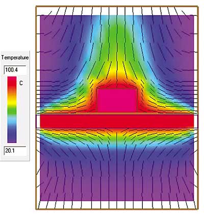
Figure 5 meanwhile shows the same set-up but using IMC as the substrate. In this scenario there is a much smaller temperature gradient, a large amount of heat spreading and a component operating temperature of 100.4°C.
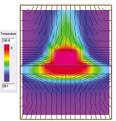 |
Figure 4. Poor heat spreading and high component temperatures using FR4.
Figure 5. The heat spreading effect achieved when using IMC.

