Introduction
When faced with the task of calculating the temperature of an IC in a package, which has an external heat sink mounted to it, a thermal engineer usually obtains a values of three thermal resistances: ΘJC , the junction-to-case thermal resistance for the package, ΘCS , the case-to-sink thermal resistance representing the thermal interface material (TIM) between the package and the heat sink, and ΘSA , the thermal resistance between the heat sink base and the ambient air. The engineer then calculates the junction temperature of the IC using the following equation [1]:
We normally think of ΘJC as being an intrinsic property of the package. We are aware that when ΘJC is measured, the package is attached to a test board. However, since pains are usually taken to minimize the loss of heat from the board during the test, we naturally assume that the details of the board construction can be neglected.
As we will explore in this column, there are exceptions to this assumption, notably when the package has two discrete paths for the heat to flow to the board: 1) from the die-mounting structure within the package, and 2) from the array of leads surrounding the die. The effect is exacerbated for packages, which have a low internal heat spreading ability.
Finite Element Analysis Calculation
A typical BGA package was chosen to demonstrate the effect in question. Its details are provided in Table 1 [2].
Table 1. Package and Board Construction
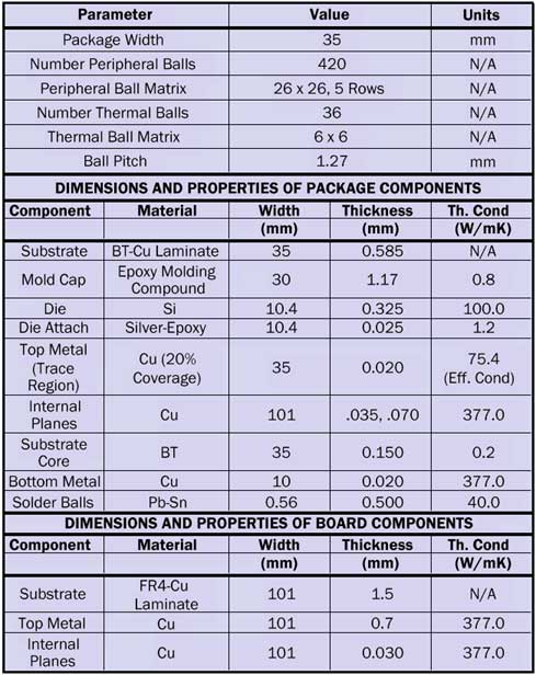 |
It was assumed to be mounted to one of two test boards: 1) a JEDEC high-conductivity test board, containing two copper planes and thermal vias [3] or 2) a low conductivity version of this board containing no planes or thermal vias.
Both the package and the board were represented with a fairly high level of fidelity to the actual design down to the via level. One simplification is that the signal traces on the package substrate were represented as a plane with thermal properties chosen to approximate the heat transfer in a trace occupying 20% of the total projected area.
A commercial finite element analysis software tool was used to perform the analysis [4]. Boundary conditions were chosen to represent an ideal ΘJC test situation, so that all the heat is extracted from the top surface of the package. A heat transfer coefficient of 40,000 W/m2K was applied to the top surface of the package to replicate the heat transfer obtained with a typical TIM layer 25�m thick, with a thermal conductivity 1 W/mK, separating the top of the package from an isothermal heat sink base. Adiabatic boundary conditions were chosen for all other package and board surfaces.
Figure 1 presents various external views of the solid model of the package and the test board. The board dimensions correspond to the JEDEC standard for area array packages [3].
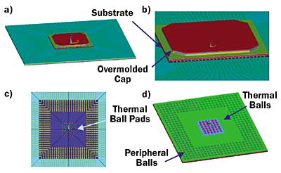 |
Figure 1. Exterior views of solid model. a) Package and test board. b) Detail of package and board. c) Detail of test board: pads and traces for peripheral balls; pads for thermal balls. d) Underside of package showing peripheral and thermal balls.Figure 2 contains a number of views of the solid model with all the dielectrics hidden; i.e., only the chip and the metal features of the package substrate and the test board are visible. Only the cases with the board containing two planes are shown. The illustrations indicate that there is a continuous metal connection between the die mounting structure down to the top plane of the board by way of thermal vias in the package and the board. The peripheral balls are connected to surface traces on the board and form a separate thermal path.
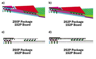 |
Figure 2. Views of 1/8 solid model with dielectric layers hidden. Packages with no and two internal planes. Test board with two planes in all cases. a) and b) perspective view. c) and d) side view.Note that in the case of the low conductivity board analyzed here (not shown), the thermal balls of the package are simply mounted to isolated metal pads on the board. Neither the thermal vias nor the planes in the board are present in the board.
Thermal Results
The thermal results for selected cases are shown in Figure 3. Figure 3a depicts the worst-case situation – a package with two signal layers and no planes (2S0P) on a board with one signal layer and no planes (1S0P). Neither the package nor the board has much ability to spread the heat beyond the die. There is a large thermal gradient in the region directly beyond the die. Here, ΘJC = 7.6°C/W, the largest value of all the cases studied.
Figure 3b provides the thermal solution with the same package, this time attached to a 1S2P board. The ability of the board to spread the heat from the region directly below the die to the region near the package periphery is evident. The heat is then able to flow upward through the package and into the heat sink. The presence of this secondary heat flow path from the die to the heat sink results in a value of Θ JC of 6.2°C/W, representing a 20% reduction, compared with case in Figure 3a.
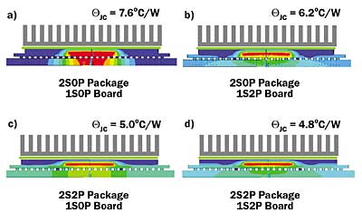 |
Figure 3. Calculated temperature contours (package cross-section). Location of heat sink and TIM indicated schematically. The 2S2P package has 70 �m thick planes.Figures 3c and 3d depict the temperature contours for a package with a 2S2P substrate, having a plane thickness of 70�m. In Figure 3c there is a 1S0P board and, in Figure 3d, a 1S2P board. An inspection, in Figure 3c, of the temperature contours in the board region near the centerline, shows the same lack of heat spreading as in Figure 3a. Conversely, the nearly isothermal temperature contours in the board region of Figure 3d indicates increased heat spreading in the board due to the presence of the two board planes. The thermal gradients in the package are similar in Figures 3c and 3d. The temperature contours in Figure 3d show a slightly larger thermal gradient in the package periphery, indicative of increased heat flow to the heat sink in that region. This observation is borne out by the calculated values of ΘJC: Figure 3c, 1S0P board, 5.0°C/W, and Figure 3d, 1S2P board, 4.8°C/W, representing a 4% reduction.
Figure 4 shows a graph of ΘJC versus the thickness of the package planes. It indicates the effect of the board construction on all of the package variants analyzed. As in the example above, the 2S2P packages manifest a fairly small impact of the board construction. The change in ΘJC due to the effect of the board varies from a low value of 6% for the package with 70�m planes to a high value of 7% for the package with 35�m planes.
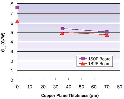 |
Figure 4. Results summary: ΘJC versus thickness of internal planes in package substrate.
Conclusions
The construction of a board can have a considerable impact on the cooling effect of a heat sink mounted to the top of a package, when a package has separate central and peripheral heat paths to the board. This effect is largest when the package has little heat spreading ability, as is found in a BGA package having a substrate without any internal planes.
These results should promote caution on the part of the thermal engineer when interpreting the results of ΘJC tests. It is important not only to understand the internal construction of a package in detail, but also to devote the same scrutiny to the boards used in testing the package as well as in the actual application.
Future Work
In a future issue, this column will deal with the use of analytical calculations to predict the effects explored here.
References
- Guenin, B., “Determining the Junction Temperature in a Plastic Semiconductor Package, Part 2,” ElectronicsCooling, Vol. 5, No. 3, 1999.
- Guenin, B., “The Many Flavors of BGA Packages,” Electronics Cooling, Vol. 8, No.1, 2002, pp. 32-40.
- JEDEC Standard JESD51-9, “Test Boards for Area Array Surface Mount Package Thermal Measurements.” Available for free download at www.jedec.org.
- ANSYS, Version 9.1.


