This topic is rather esoteric and usually an afterthought in commercial and industrial applications. In military and defense electronics, it is one of the major drivers for design and product architecture early on in the design cycle with specific targets/budgets. As with junction temperature requirements in a thermal design, there are structural dynamic issues that need to be addressed up front to ensure successful completion of a program. Mil handbook 810 [1] among other specifications drives the requirements, qualification and verification of hardware. The equivalent on the commercial side would be specifications and tests established by NEBS (Network Equipment Building System), Telcordia, etc.
The commercial product development cycle is continually shrinking and any redo of a printed circuit board (PCB) would delay product release by at least a few months. Typical challenges facing packaging engineers are signal integrity, component placement, EMI/RFI (electromagnetic and radio frequency interference), thermal management and similar design issues. PCB structural dynamics is not typically looked into and is often addressed only after a failure has occurred. However, this is changing slowly as the increasing thermal loads necessitate the use of bigger heat sinks with more convective heat transfer capacity. The sheer size and mass of these heat sinks induce deflections that can wreak havoc on the solder balls of typical high power chips.
Case in Point
A massive heat sink with a span of 76 to 127 mm is mounted (suspension design) on a BGA (Ball Grid Array) chip with a footprint roughly 30.5 x 30.5 mm located in the center of a 305 x 381 mm PCB. The question to be asked relative to vibration is: How would this affect board dynamics vis-a-vis NEBS, transportation, seismic and similar specifications and what provisions can be made to mitigate, if not eliminate the redo of the board caused by local solder joint failure? Although the specifics of heat-sink/suspension-backer plate design would also be of interest they are beyond the scope of this article. To put things in perspective we will consider what random vibration is and then follow the step-by-step approach outlined below to solve this problem. For the purpose of clarity, a simplified explanation is being used.
Solution Steps
1) Calculate energy input to the PCB
2) Approximate natural frequency of a printed circuit board
3) Approximate PCB transmissibility
4) Approximate “system” response, i.e. Grms OUT
5) Approximate deflection based on the above
Understanding Random Vibration
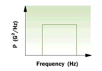
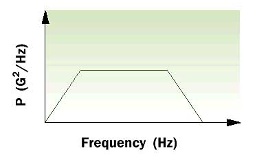
Random vibration is specified for acceptance tests, screening tests and qualification tests as it more closely represents the true environment in which electronic equipment must operate. Random vibration is nonperiodic with all of the frequencies within a given bandwidth present all the time, and at any instance of time. This means that over a frequency bandwidth of 20 to 2000 Hz, all of the structural resonances within the same bandwidth, at the box, board and component levels, will all be excited at the same time. This helps to identify failures that can not be duplicated in a sinusoidal environment. This “random” feature is frequently referred to as white noise. The probability of a given instantaneous acceleration follows the Gaussian distribution curve. Typical white noise curves are shown in Figure 1.
 |
Figure 1a. White noise input curve with constant input PSD.
Figure 1b. White noise input curve with positive and negative slopes.
1) Input Energy to the System
The input energy to the system is simply the square root of the area under the curve which leads to:
2) Natural Frequency of a Printed Circuit Board
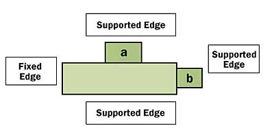
There are a variety of printed circuit boards manufactured in the electronic industry today. Epoxy glass is the most common material with laminated layers of copper. The rectangular shape is easily adopted and facilitates “plug and play” troubleshooting and manufacturing. The manner in which PCBs are supported determine their dynamic response. Three scenarios are possible: 1) free edge; 2) supported edge; and 3) fixed edge. The natural frequency of a PWB can be approximated as a plate problem.
 |
Figure 2. Representation of a typical telecom blade.Figure 2 represents an example of a typical telecom blade with three sides supported and one fixed . A number of references [2-5] may be found outlining flat plate relationships such as that in Equation (2) which may be used to estimate natural frequency, fn, of a flat plate.
 |
whereD is the plate stiffness factor
ρis the density
a is the length of the plate
b is the width of the plate
3) Approximating PWB Transmissibility
It has been shown empirically that the transmissibility, Q, of a printed circuit board is proportional to square root of the natural frequency:
where C is a constant with a value typically between 0.5 to 2 depending on board size. For example if fn= 200 Hz, Q may be approximated as
4) Approximating “System Response”
The “system response” may be approximated using equation (4) which estimates the RMS response of the mass to a broad band vibration.
where
P is the input PSD in units of G2/Hz at the resonant frequency
fn is the resonant frequency, Hz
Q is transmissibility at the resonant frequency
For the above example:
5) Approximating PCB Deflection
Treating the printed circuit board as a single-degree-of-freedom system, the dynamic deflection at resonance may be approximated by
 |
For the above example:
Once an approximation of deflection is made, it should be checked against the design limits. In order to reduce deflection, stiffness of the board has to increase. This is usually done via stiffeners, additional anchor points, snubbers, and other mechanical means. In order to reduce stresses on PCBs or various devices on them the general guideline is to “decouple” hardware by one octave, i.e., 20, 40, 80, 160, and so on. For instance, the relationship between the chassis to board to a heat sink/bracket should follow the above multiplier. This helps mitigate any potential coupling between various constituents of the box.
References
- www.dtc.army.mil/pdf/810.pdf
- Steinberg, D.S., Vibration Analysis for Electronic Equipment, John Wiley and Sons, New York, 2000.
- Sloan, J.L., Design and Packaging of Electronic Equipment, Van Nostrand Reinhold Co., New York, 1985.
- Matisoff, B.S., Handbook of Electronics Packaging Design and Engineering, Van Nostrand Reinhold, New York, 1990.
- Young, W.C. and Budynas, R.G., Roark’s Formulas for Stress and Strain, McGraw-Hill, New York, 2002.


