Introduction
Integrated circuits range in power consumption from mW (or maybe microwatts) to hundreds of Watts with the number of electrical connections to the next level packaging ranging from eight to over 1,000. With such a broad range of interesting packaging to consider, it is no wonder that any simple generalizations will always find exceptions. This review article will attempt to describe the most common thermal enhancements currently available. For this article, the number of connections of the package to the next level interconnect (the printed circuit board) are abbreviated as i/o for input/output. For this discussion, the i/o count will include the power and ground connections.
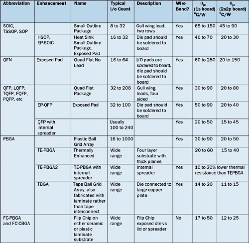 |
Table 1. List of Common Integrated Circuit PackagesThe data in Table 1 list the typical range of Junction-to-Ambient Thermal Resistance (θja) observed for some common integrated circuit packages. As a method of comparing and describing the thermal performance of the packages, the standard thermal resistances as defined by JEDEC are used [1]. A guideline and short tutorial on the use of the resistances and the specifications is found among the JEDEC documents [2]. Both the qja values determined on a single layer (1s) board and on a four metal layer (2s2p or 2 signals and 2 planes) board are provided. The thermal test boards are also specified in this series of specifications [3]. The readers of this publication should recognize the limitations of using standard thermal resistances in estimating thermal performance.
The list of packages in Table 1 omits a number of specialized packages including PGA (Pin Grid Array Packages), SIP (Single Inline Power Packages), ceramic and plastic DIP (Dual Inline Packages), ceramic BGA (Ball Grid Array) packages, CLCC (Ceramic Leadless Chip Carrier) and all the chip scale and direct chip attach configurations.
The package choice is driven by the number of i/o connections required, electrical performance (inductance or controlled impedance), power delivery design, thermal requirements, customer demand (matching of previous products) and cost. For this discussion, we will consider three groups of packages:
- low lead count with low cost requirements
- medium i/o count packages
- high electrical performance flip chip packages
Low Lead Count Packages
The thermal performance of the SOIC (Small Outline Integrated Circuit) and QFP (Quad Flat Package) style package (Figure 1) is determined to a large extent by the package size, the leadframe pad for the die (commonly called the die pad or flag) and die size. To improve the mechanical integrity of the package during a board soldering process, the leadframe pad size is normally minimized.
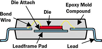 |
Figure 1. SOIC or QFP cross section.The first enhancement that is used for these packages is a “thermal lead” or “fused lead”, which is a lead that is connected to the flag. This provides a direct thermal path from the flag to the printed circuit board. Because of the need to tool a special leadframe for each device, this enhancement is not common. Recently, exposed pad versions of this package have been used (Figure 2). By allowing the leadframe pad to be soldered to the printed circuit board, much improved thermal performance of the package is obtained. For instance, a 64 10 x 10 EP-LQFP (Exposed Pad – Low Profile Quad Flat Package) with a die size of 4.4 x 3.7 mm had a θja in natural convection on a 2s2p board of 26°C/W compared to 47°C/W for the standard package.
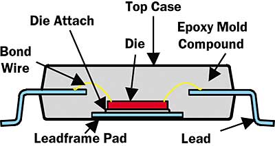 |
Figure 2. EP-SOIC or EP-QFP with the die attached to a pad visible from the bottom of the package.One would normally model SOIC and QFP packages with two resistor models if a more detailed model is not available. Two resistor models can be created from the θjb (Junction to Board Thermal Resistance) and θjc (Junction to Case Thermal Resistance) [2]. For the exposed pad package soldered to the printed circuit board, adequate accuracy can usually be obtained by modeling the thermal resistance from the die to the printed circuit board. To create such a model, it is important to ask whether the component supplier is providing the θjc to the exposed pad of the package rather than the top of the package.
For the exposed pad package to achieve the performance indicated by the θja (on 2s2p board) that is quoted by the component supplier, it is important that there is an array of vias under the exposed pad and that the vias are connected to one or more planes in the printed circuit board. The specification of the device should be documented to show whether the exposed pad can be electrically connected to the ground or to one of the power planes. When planes are not available, it is common practice to couple the exposed pad to a large metal “radiator” pad (perhaps 25 x 25 mm or larger) on the other side of the printed circuit board. Another thermal enhancement for QFP packages is an internal spreader. Because the thermal interface is rarely well controlled between the leadframe pad and the spreader, there can be a considerable range in thermal performance.
Because of the relatively thick mold compound layer between the die and the top surface of the package, the junction-to-top case thermal resistance of the package is relatively large. Still, heat sink attachment with adhesive thermal tapes is occasionally used. The thermal performance improvement with such a heat sink is relatively limited.
Medium i/o Count
The wire bond PBGA (Plastic Ball Grid Array) package shown in Figure 3 is the most common package type used for the medium i/o count devices. Again, the package choice is driven by cost (wire bond substrates are cheaper than flip-chip substrates because of the lower connection density), relative high density of i/o and better electrical performance than large leaded packages. The package size is frequently driven by the ball grid array pitch. Obviously, the package with the balls on 1.27 mm pitch is much larger than the same number of balls on a 0.5 mm pitch. As a general rule, the cost of a package substrate and the printed circuit board scale with area; larger area equals higher cost. But, finer (smaller) pitch parts increase the cost and complexity of both the laminate substrate of the package and the cost and complexity of the printed circuit board. In many cases, the use of 0.5 mm pitch balls will require a high density interconnect (HDI) printed circuit board, which is much more expensive than standard printed circuit board technologies. Having more connections in a small area also increases the layer count in the printed circuit board. For general use, the most common pitch seems to be 1 mm.
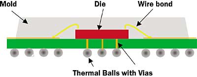 |
Figure 3. Wire bond PBGA package with two metal layers in substrate.The most important variable in the thermal performance is the die size and whether there are vias and balls under the die. The package is commonly modeled as a two resistor model using the θjb and θjc provided by the component supplier if a more detailed model is not available. It is also important to consider how the package connects to the printed circuit board. The thermal balls and ground balls should connect to the ground plane in the printed circuit board with one via per ball. Significant degradation of the thermal performance can occur if the ground balls are not connected to the planes. One example was an eight layer test board with only a few vias connecting the thermal balls to the ground plane. On this board, the package had a natural convection θja of 47°C/W compared to 29°C/W determined on the 2s2p standard thermal board [3]. The board conduction and connectivity to the package is extremely important to the performance of the device.
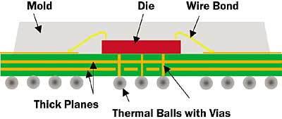 |
Figure 4. TEPBGA with thick internal planes in the substrate.The two common thermal enhancements on PBGA packages are frequently called TE-PBGA (Figure 4) and TE-PBGA2 (Thermally Enhanced Plastic Ball Grid Array Package; the 2 indicates a spreader) (Figure 5). The TE-PBGA is normally constructed with two inner metal planes in the package substrate. Frequently those metal planes are 2 oz (about 65 microns) thick. The thermal performance improvement of those planes is determined by the connectivity of the planes. The power plane is frequently segmented to allow different supply voltages. This approach often eliminates the thermal spreading, which would occur in a continuous plane. The extreme example is a four metal layer substrate with the internal layers used for routing with the buried vias through the central core. Such a four layer substrate design may have worse thermal performance than a two layer design with vias through the entire substrate.
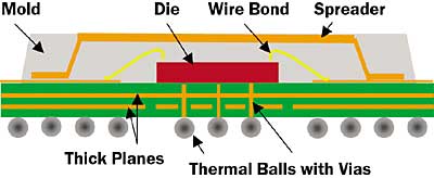 |
Figure 5. TE-PBGA2 contains thick internal planes in the substrate and a spreader.
Note that the spreader is separated from the die by the mold compound.The next level of thermal enhancement is the addition of a thermal spreader in the package. The exposed metal layer on the top of the package does not mean vastly better thermal performance; typically the reduction in thermal resistance due to the spreader is of the order of 10 to 20%. Table 2 gives an example of the type of thermal performance that is observed with the TE-PBGA and the TE-PBGA2. In this table, the Ψjt (junction-to- package top thermal characterization parameter [2]) is also provided.
 |
Table 2. Measured Thermal Performance of 516 27×27 mm PBGA with 5.7×6.2 mm DieThe TE-PBGA and TE-PBGA2 do not have low junction-to-case thermal resistances because of the mold compound between the die and the top of the package. As a result, adding heat sinks improves thermal performance, but not as much as might be desired. For instance, for the 516 27 x 27 mm TE-PBGA2 referenced above, adding a 41 x 43 x 16 mm extruded, cross cut pin fin heat sink in natural convection lowered the thermal resistance of the device on a 2s2p test board from 19°C/W to 12°C/W.
The other common high thermal performance wire bond ball grid array package is the TBGA (Tape Ball Grid Array) (Figure 6) or similar package with laminate based connections rather than the tape based connections. The die is face down with the back of the die bonded to the metal spreader. Because there are no balls in the center of the array, the TBGA package is larger than a corresponding PBGA. The copper spreader and its large size produces good thermal performance. The low thermal resistance from the die to the spreader (case) causes a low junction-to-case thermal resistance, which means that a heat sink can increase the power handling capabilities of the device considerably. The junction-to-case thermal resistance is die-size dependent. The flatness of the back of the case must be considered when determining the best thermal interface material for use with a heat sink.
 |
Figure 6. TBGA – die down wire bond package with die
adhesively attached to copper spreader.
Flip Chip Packages
Flip chip packages are the preferred choice when the best electrical performance is necessary for high i/o devices. Flip chip packages are used over a range of power dissipations from less than 1 W to over 100 W.
Table 3. Measured Thermal Resistance for Three Substrate Types for Flip Chip
360 25×25 mm DeviceFigure 7 shows a pictorial view of a bare die flip chip package. For low power devices, the standard thermal resistances for the package are useful as a guide to their performance. Table 3 provides the thermal resistance of a 360 i/o, 25 x 25 mm, exposed-die flip chip package with three different substrate materials. It is interesting to contrast the two different ceramic substrates. The high temperature cofired substrate with approximately 90% alumina has a conductivity of approximately 16 W/m-K. The metallization is either tungsten or other glass frit composition with low enough conductivity that the metallization patterns do not significantly improve thermal performance of the package. The HiCTE (High Coefficient of Thermal Expansion) ceramic is a low fired ceramic with a higher glass content and much lower thermal conductivity, usually about 2 W/m-K, but uses copper metallization. The copper content must be considered when determining the conductivity of the substrate. The third common style of substrate is a plastic laminate, usually consisting of a laminate core such as BT laminate with large drilled vias and buildup layers of dielectric and plated copper. The vias in the buildup layers are usually much smaller diameter and constructed by photolithography or by laser ablation. At higher powers, most of the heat transfer will be through a heat sink. Hence, the standard junction to ambient or junction to board thermal resistances are almost irrelevant. The relevant thermal metric is θjc.
 |
Figure 7. Flip chip package without a lid.
Summary
This article has described some of the common integrated circuit packages and some available thermal enhancements. While the article has focused on an overview of the internal details of the packages, the ultimate package thermal performance depends on the application environment. The system level design must be configured to take advantage of the thermal enhancements to meet the expected performance. As an industry, we are progressing toward better vendor data, better component supplier data and improved simulation tools. We encourage you to be involved in that process through the JEDEC JC15.1 committee and through the industry technical conferences, such as Semi-Therm and ITherm, and through publications, such as ElectronicsCooling.
References
- JESD51 series of specifications, “Methodology for the Thermal Measurement of Component Packages (Single Semiconductor Device),” available for downloading at www.jedec.org.
- JESD51-12, “Guidelines for Reporting and Using Electronic Package Thermal Information,” available for downloading at www.jedec.org.
- Thermal test board specifications include JESD51-3, JESD51-5, JESD51-7 and JESD51-9, JESD51-10 and JESD51-11, available for downloading at www.jedec.org.


