Introduction
It comes as no surprise to anyone in our industry that device power levels are increasing to support customer expectations of ever greater functionality and performance. The greatest thermal challenges in computing occur in the packaging of processors. This results not only from the fact that processors typically have the largest overall power dissipation in a system, but that they have the highest heat flux, localized in what are commonly called “hot spots”.
The processor architects of the world have not been asleep at the wheel while power levels continue to increase. They are developing lower frequency multi-core, multi-thread processors, which exploit parallelism in computer code to perform the same compute workload as a higher frequency single core chip, but with lower power consumption.
Nevertheless, the 2005 International Technology Roadmap for Semiconductors (ITRS) indicates a continuing rise of high performance processors from a maximum power of 365 W in 2006 to 515 W by 2011 [1]. Furthermore, this roadmap predicts a decrease in the maximum allowable junction temperature from 100°C, currently, to 90°C by 2011. All this points to the continued need for development of higher performance thermal management solutions for these chips.
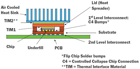 |
Figure 1. Diagram of a flip-chip IC in a high-performance package with attached heat sink.Figure 1 depicts a typical configuration for a flip-chip processor attached to an external heat sink, which is usually air cooled. The temperature of the chip depends upon both the package and the heat sink thermal performance. This article will focus primarily on the thermal performance of the package.
The main heat flow path from the chip to air is: Chip => TIM1 => Lid => TIM2 => Heat sink => Air. The package contribution to this path is determined by the thermal conductivity of TIM1 and of the lid. Advances in the thermal performance of processor packages are ultimately determined by innovations in materials for these components.
There is a synergy in the choice of materials for the TIM and the lid. In order to achieve enhanced thermal conductivities, manufacturers have been substituting metallic particles in thermal greases and gels for the traditional ceramic ones. In order to achieve even higher levels of thermal conductivity, it is necessary to use a TIM1, which is 100% metal, namely a solder [2]. This places further demands on the lid materials. Not only must they have a high thermal conductivity, but also their coefficient of thermal expansion (CTE) has to be a reasonably close match to silicon in order to maintain the integrity of the solder joint over many thermal cycles. Unfortunately, nature has not given us a high conductivity metal whose CTE approximates that of silicon.
However, materials science has given us composite materials, which can achieve a high thermal conductivity, while controlling the CTE. These composite materials consist of metal, ceramic, or polymer matrix, loaded with high conductivity particles or fibers. The composite materials with the highest thermal conductivities contain either diamond or graphite particles or graphite fibers [3]. The best materials have a thermal conductivity in excess of 1000 W/mK. Some are isotropic. Others are orthotropic and have a through-thickness conductivity, kZ, which is as much as a factor of 10-100 less than the in-plane conductivity, kX-Y.
This article will present the results of thermal simulations, which explore the relationship between the thermal conductivity of TIM1 and lid materials on the die temperature for a processor of moderate power. Also, it will investigate a very high heat flux situation and a possible die-level thermal solution.
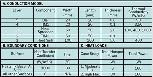
Table 1. Assumptions of simulation
 |
Simulation Assumptions
The simulation only includes the five components in the major heat flow path discussed above. The component dimensions and the values of thermal conductivity are presented in Table 1. (Note that the values of k assumed for the TIMs are effective values, which are lower than the bulk value of k, due to the presence of an interfacial thermal resistance [4]. Note also that the thermal conductivity chosen for silicon assumes a temperature 160°C, which is in the middle of the range of calculated hot spot temperatures.) The calculations were performed at several values of the thermal conductivity of TIM1 and the heat spreader. A single value of thermal conductivity was used for each of the other components in all of the calculations. The configuration with the lowest conductivity values for TIM1 and the lid is referred to as the baseline case. All five conductivities represent typical values for today’s mainstream high-performance applications. Here the actual materials would be a metal-filled grease for TIM1 and TIM2, copper-infiltrated tungsten for the lid, and a solid copper heat sink base. The second, higher value of kTIM1 is representative of a solder.
The model was further simplified in that the heat sink base is represented as a solid in the model, but not the fins. Their presence is represented by an enhanced heat transfer coefficient applied to the fin side of the heat sink base. All other surfaces are assumed to be adiabatic. The ambient air temperature was assumed to be 30°C.
As mentioned, the challenge of cooling processors is not only dealing with their total power, but also with the hot spots. The power map, on actual processors, can be very complicated. However, the essential physics of the heat transfer from a high power IC can be captured by using a very simple power map consisting of 2 hot spots on a background of uniform heat flux applied to the surface of a silicon chip [5].
The hot spots are each 2 x 2 mm2 and separated by 6 mm, center to center. Two different heat flux regimes are examined: 1) the power applied to each hot spot is equal to 4 W providing a heat flux of 100W/cm2; 2) the power applied to each hot spot is 40 W. The heat flux in this case is the extreme value of 1000 W/cm2. In both cases, there is a uniform flux applied to the remainder of the chip surface and the total power is 160 W. Temperature contours were calculated using a commercial Finite Element Analysis program [6].
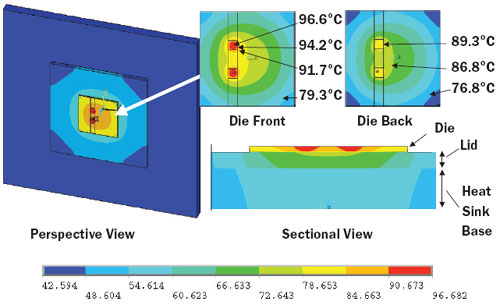 |
Figure 2. Calculated temperature contours superimposed on a FEA solid model. The temperature scale applies to the perspective and sectional views. The close-ups of the die front and back have a magnified temperature scale as indicated by the labels.
Simulation Results
Moderate Hot Spot Heat Flux
Figure 2 depicts temperature contours on the solid model of the chip and other components for the baseline case. Viewing the front surface of the chip, one sees a temperature peak at the center of each hot spot region. The calculated peak die temperature is 96.7°C. This provides a bit of margin compared with the current ITRS value for maximum junction temperature.
The surface temperature quickly drops off with increasing distance from the hot spot center (a drop of 5°C at a distance of 1 mm away from the center). The temperature contours at the back side of the die show a significant reduction of the thermal gradients. There the contours become more circular. A similar view of layers deeper into the package/heat sink stack would show an almost complete circularization of the temperature contours.
Comparing the temperature contours at the front and back of the die indicate that that there is approximately a 7°C temperature difference between the maximum temperatures on these two surfaces. This temperature difference is intrinsic to the silicon and is independent of the composition of the other layers in the package.
The cross-sectional view shows the progression from the contour map at the die front to that at its back side. The deeper layers of the package/heat sink stack show an abrupt change in temperature at both TIM regions due to the comparatively lower thermal conductivity of the TIM materials compared with that of the other components.
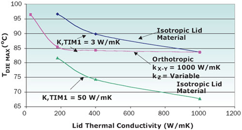 |
Figure 3. Thermal simulation results, indicating the effect on die temperature of kTIM1 and kLID for isotropic and orthotropic lid materials.Figure 3 contains a graph of the maximum die temperature versus the lid conductivity, exploring two major effects: 1) the variation in the thermal conductivity of TIM1 for an isotropic lid material and 2) the replacement of an isotropic lid with one with orthotropic thermal conductivity, representative of certain composite materials. For the isotropic materials, changing the TIM from a high-conductivity grease to a solder lowers the peak die temperature by about 15°C independent of the lid thermal conductivity. Increasing the lid thermal conductivity from the baseline value of 180 W/mK to the maximum value of 1000 W/mK further lowers the peak die temperature by about 14°C to 68°C. Together, these effects reduce the die temperature rise relative to the ambient temperature by 43%.
The situation with the orthotropic material is quite different than that with the isotropic one. With kX-Y and kZ equal to 1000 W/mK, the die temperature, of course, is the same as for the isotropic lid with a k equal to 1000 W/mK. Decreasing kZ to a value of 180 W/mK increases the die temperature by less than 2°C. However, decreasing kZ below 180 W/mK, produces a rapid rise in chip temperature. As kZ is decreased to 25 W/mK, the chip temperature is nearly identical to the value achieved with an isotropic heat spreader with the baseline thermal conductivity. These results suggest that the thermal engineer should not simply focus on the headline in-plane thermal conductivity of an orthotropic material, but should pay particular attention to the normal component of thermal conductivity.
Extreme Hot Spot Heat Flux
It was mentioned above that 7°C of the total temperature rise of the chip was within the silicon itself, and is unaffected by the other material choices in the package stack. It is an interesting exercise to envision what thermal solutions would apply if the heat flux was increased by a factor of 10 to 1000 W/cm2, achieved by applying 40 W to the same 2 x 2 mm regions as before. Admittedly this is an extreme level of heat flux. However, experience tells this author that if a thermal management solution were practical, the processor architects would take advantage of it to further increase chip performance.
At a heat flux of this magnitude, the 7°C front to back temperature difference in the chip would become 70°C. Even with the highest conductivity package components, it would require sub-ambient cooling to keep the junction temperature below the target value of 100°C. To implement a thermal management solution involving refrigeration would not only greatly increase the initial hardware cost, but would be accompanied by an increase in power consumption, an ongoing cost.
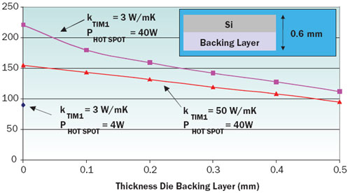 |
Figure 4. Thermal simulation results, for silicon chip bonded to high thermal conductivity (1000 W/mK) backing material at varying thickness and kTIM1. As indicated by the inset, the total thickness of the silicon + backing material remains constant.The optimum thermal solution would be to significantly reduce the excess temperature rise within the silicon, thereby eliminating the need for refrigeration. Figure 4 presents the results of a simulation, which assumes that the silicon is covalently bonded to a backing material with a thermal conductivity of 1000 W/mK. It is assumed that the thickness of the chip + backing layer = 0.6 mm, the same as the chip thickness in the first study. The simulation explores the effect of varying the thickness of the backing layer from 0 to 0.5 mm. This would, in effect, be replacing an ever greater fraction of the chip thickness with a material with over 10 times its thermal conductivity.
Note that the total chip power is assumed to be 160 W as in the earlier study. Therefore, the calculated increase in peak chip temperature is due only to the effect of the increased flux in the hot spots.
At zero thickness for the backing layer, the chip temperature is 221°C with the grease TIM1 and 151°C for the solder TIM1. The solder causes a significant reduction in the chip temperature, but, as expected, the chip is still much too hot. The curves indicate that increasing the backing layer thickness produces a significant reduction in the chip temperature.
The calculated chip temperatures at the greatest backing layer thickness of 0.5 mm (and thinnest silicon thickness), are much reduced, at 112°C and 95°C, respectively for the grease and solder TIM1. In spite of the extreme value of heat flux, the latter chip temperature is lower than the target value of 100°C and is nearly equal to the chip temperature in the baseline case.
Using this sort of strategy not only would reduce the chip temperature significantly, it also diminishes the sensitivity of the chip temperature to the thermal conductivity of the TIM1 layer.
It should be pointed out that, while this approach is not used commercially for silicon, a version of it is standard practice in high power gallium nitride semiconductors. Here the GaN thickness is on the order of 1-2 microns and is epitaxially grown on crystalline silicon carbide, which has a thermal conductivity about 3 to 4 times that of GaN.
Conclusions
A series of simulations were performed to explore the effect of different material choices for the TIM1 and lid components of a flip-chip package. In spite of the increasing power roadmap for processors, there are advanced material options available today that allow much of the expected power increase to be dealt with at the package level.
Beyond today, there is the possibility of much more significant improvements in package level thermal performance by the integration of advanced thermal materials at the wafer level itself.
References
- International Technology Roadmap for Semiconductors, 2005 Edition. Available for free downloading at http://www.itrs.net/Common/2005ITRS/Home2005.htm.
- Viswanath, R., Wakharkar, V., Watwe, A., and Lebonheur, V., “Thermal Performance Challenges from Silicon to Systems,” Intel Technology Journal, Volume 4, Number 3, 2000.
- Zweben, C. , “Revolutionary New Thermal Management Materials,” ElectronicsCooling, Vol. 11, No. 2, May, 2005.
- Guenin, B., “Calculations for Thermal Interface Materials, ElectronicsCooling, Vol. 9, No. 3, August 2003.
- Xu, G., Guenin, B., and Vogel, M., “Extension of Air Cooling for High Power Processors,” Proceedings, Ninth Intersociety Conference on Thermal and Thermomechanical Phenomena in Electronic Systems (ITherm), June, 2004.
- ANSYS, V 9.0.


