Introduction
The same trend that has led to ever-higher levels of integration of computation and processing functions on a single chip is now driving the integration of several chips into the same package. The use of multi-chip packages (MCPs) enables miniaturization of a circuit when it is not practical to incorporate all of the desired functionality on a single chip.
The proliferation of MCPs has posed a number of challenges to the thermal engineering community. In the area of package characterization, it is pushing this community beyond its comfort zone of thermal resistances (Thetas) into a new realm that is still unfamiliar to many.
In the more familiar territory of single chip packages (SCPs) the use of single parameter thermal metrics, such as ΘJA, ΘJC. and ΘJB (representing, junction-to-air, junction-to-case, and junction-to-board thermal resistances, respectively) provide an intuitively simple means of calculating the junction temperature of a chip with respect to an appropriate reference temperature [1]. These metrics function in a manner exactly analogous to an electrical resistance. The difference between the junction temperature, TJ and a reference temperature, TX, depends only on the power dissipated in that particular chip and the value of the appropriate thermal metric, represented here in a generalized format, ΘJX.
This is simplicity itself. It is an approach that even non-thermal engineers have grown comfortable with. Life, unfortunately, is more complicated in dealing with MCPs.
 |
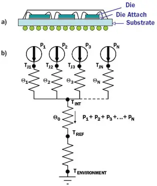
Figure 1(a) Concept drawing.
Figure 1(b) Simplified thermal circuit diagram for a lateral Multi-chip Package.
The Physics of Heat Flow in a Lateral MCP
This article will focus on a “lateral” MCP, namely, one in which all the chips are located in the same plane. Another family of MCPs, namely those employing stacked chips, is also popular, but that is another discussion. The reader is referred to a previous column on this subject for a comparison of lateral and stacked MCPs [2]. Figure 1 illustrates a lateral MCM and a simplified thermal resistance diagram that captures the essential physics of heat flow and temperature variations within the package. It shows the heat from all the chips flowing into a common region, usually internal to the package, with temperature TINT. TINT is a function of the total heat generated collectively by all of the chips. Each chip experiences a further temperature increase with respect to TINT, which is proportional to the power applied to that particular chip. Even when a chip is not powered, its temperature will be elevated by the power applied to the other chips. Hence, the temperature of any of the chips is a function of the power applied to all of the chips. This is an inescapable reality in the thermal analysis of MCPs. (Note: The thermal resistance diagram is intended to illustrate the heat flow paths and not to be rigorous. For example, it does not account for the thermal gradient in the common region.)
Fortunately, there is a well-established method in heat transfer that uses the principle of superposition to calculate the temperature of all of the chips at an arbitrary combination of power levels applied to the chips [3,4]. The superposition method can be applied both to experimental testing as well as to thermal models. Its use with a 3-D thermal model is demonstrated in the next section.
Application of the Principle of Linear Superposition
The method is described below for a four-chip package. It is assumed here that any non-linear effects (power- and temperature-dependent) are small.
The method consists of sequentially powering up each chip to a fixed power, assumed here to be 1 W, while maintaining the other chips at zero power and measuring the temperature rise of each chip. The influence coefficients, Fij, represent the effect of power applied to the ith chip on the temperature of the jth chip. This method is indicated symbolically for first two steps of this process:
 |
Once the influence coefficients are determined in this way for all four the chips, the temperature rise of any chip may be calculated for an arbitrary power combination using the following equation
This equation is simply a reflection of the fact that, in a linear system, the increase in the temperature of, say, the second chip, caused by the power applied to the first chip, is independent of the power applied to the other chips. Furthermore, this temperature increase is proportional to the power applied to the first chip.
While not as simple as using Equation 1, the above equations, extended to account for all the chips, can easily be dealt with using a spreadsheet. It does complicate the issue of data transfer from the package supplier to the user in that a matrix of influence coefficients would be needed rather than a single parameter. It is easy to envision an electronic transfer of the matrix into a simple software tool to allow the convenient calculation of the MCP chip temperatures for specific power levels of interest to the thermal engineer.
In application environments that are dominated by natural convection or radiation cooling, this simple formalism must be supplemented by an additional term, which is a function of the total power applied to all chips due to the temperature dependence of these boundary conditions [3,4].
Thermal Simulation of a Lateral MCP
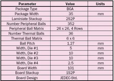
In order to demonstrate the application of the linear superposition method, a Finite Element Analysis (FEA) calculation was performed for a four-chip Ball Grid Array (BGA) package attached to a JEDEC-standard test board [5]. The basic construction parameters of this package, the board, and the sizes of the four chips are provided in Table 1. The layer thicknesses, material choices, and assumed values of thermal conductivity for the package and the board are the same as those reported in a previous column [6]. The reader with an interest in those specific aspects of the model is referred to that column.
Table 1. Package and Test Board Construction
 |
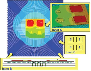
Figure 2 depicts the solid model of the package and board. The package laminate has a 2S2P stackup with two outer signal layers and two internal planes. The board has a 1S2P structure. Each chip is in good thermal contact with the top metal plane through an array of vias, which are represented in the model as a cuboid with an appropriately chosen value of effective thermal conductivity. Thermal vias in the package and board serve as a significant heat flow path from the top plane of the package to the top plane of the board. The board planes enhance the heat transfer to the air by spreading the heat to the board extremities.
 |
Figure 2. Calculated temperature contours superimposed on a FEA solid model of 4-chip MCP attached to a JEDEC-standard test board. Insets A and B show the model with dielectric layers hidden. Inset A: perspective view of chip locations. Inset B: side views showing metal layers and via structure in the package and board. Inset C provides the numbering convention for the chips.The thermal problem was solved using a commercial FEA tool [7]. A constant value of heat transfer coefficient of 10 W/m2K was applied to all external surfaces of the package and the board. All values of thermal conductivity were assumed to be constant. These assumptions make the thermal model perfectly linear.
The FEA problem was solved for a total of nine combinations of power applied to the chips and both the average and maximum temperature calculated for each chip. The various power combinations and the calculated values of chip temperature are reported in Table 2.
Table 2. Junction Temperature Rise Calculated By FEA Model
 |
The power inputs and temperature outputs of the “training exercise” to calculate the influence coefficients for average and peak die temperatures are represented in Conditions 1-4.
The above treatment of the superposition method in Equations 2-4 intentionally sidestepped the more formal matrix notation to emphasize the relative simplicity of the method. However, it should be noted that the three 4 x 4 arrays in the training exercise for the power, average die temperature, and maximum die temperature have precisely the format of the power matrix and influence coefficient matrices.Conditions 5-9 represent a series of arbitrarily chosen power combinations applied to all four chips. FEA solutions were generated using each combination and are reported in Table 2 as before. The superposition method was applied to these same power conditions using the appropriate influence coefficients to calculate both the average and maximum chip temperatures.
The lower part of Table 2 indicates the error in the superposition method calculations using the FEA results as the baseline. For the results involving the average die temperatures, the error is typically less than less than 0.04% in all cases – a dramatic confirmation of the power of this method. (Note that these small errors are the result of convergence and numerical precision in the calculations and not directly attributed to the use of superposition in a linear model.) In contrast, the error for calculations based on the maximum temperature of each of the chips is much greater and is as large as 3%. In this case, the error values all have a plus sign, indicating that the superposition method results are consistently larger than the FEA results. It must be noted that an error of 3% is very acceptable for most electronic applications and that it is common practice to report chip temperatures in terms of the maximum value.
The results clearly indicate that, once the influence coefficients are known, the task of calculating chip temperatures for an MCP at an arbitrary power combination can be both a relatively simple and accurate process.
Conclusions
The changing landscape of packaging has created the need for many more thermal engineers to get involved in the use of multi-chip packages. Clearly, dealing with MCPs requires adopting a different vocabulary and different analysis methods. As is shown here, once the influence coefficients are known, predicting chip temperatures can be a straightforward affair. The challenge will be in adapting single chip package testing and modeling techniques to deal with the added complexity of MCPs in generating these coefficients.
References
- JEDEC document JESD51-12, “Guidelines for Reporting and Using Electronic Package Thermal Information,” available for download at www.jedec.org.
- Guenin, B., “Thermal Calculations for Multi-Chip Modules, ElectronicsCooling, Vol. 8., No. 4, November 2002.
- Lall, B., Guenin, B., and Molnar, R, “Methodology for Thermal Evaluation of Multichip Modules,” IEEE Trans. Comp., Packaging, Manuf. Technol. – Part A, Vol. 18, No. 4, December 1995, pp. 758-764.
- Zahn, B.,”Steady State Thermal Characterization of Multiple Output Devices Using Linear Superposition Theory and a Non-Linear Matrix Multiplier,” Proceedings SEMI-THERM XIV Conference, March 1998, pp. 39-46.
- JEDEC Standard JESD51-9, “Test Boards for Area Array Surface Mount Package Thermal Measurements,” available for free download at www.jedec.org.
- Guenin, B., “A Funny Thing Happened On The Way To The Heatsink,” ElectronicsCooling, Vol. 11, No. 3, August 2005
- ANSYS®, Version 10.0.


