Introduction
This Calculation Corner continues Part I, published in the previous issue [1]. Part I described the construction of a typical flip-chip package configuration for high-power chips, consisting of a laminate assembly of materials adhesively bonded together and having different Coefficients of Thermal Expansion (CTE). The process of bonding these different materials together involves heating the package. During cool-down, once an adhesive layer stiffens (due to either curing or solidification), subsequent cooling causes stress transmission between the layers and warpage of the package.
Without proper selection of the package materials, the strain produced by temperature changes can lead to failure of an adhesive joint or to fracture of one or more of the package components. The present article attempts to provide insight into the package warpage process, which drives these failure modes. It presents the results of Finite Element Analysis (FEA) simulations of the warpage of a Si die, flip-chip-attached to a substrate, compares them to the results of a simple analytical calculation, and explores their implications for package design.
Thermal-Mechanical Analysis
Warpage calculations were performed for two simple configurations.
- 2-layer structure consisting of a silicon chip bonded directly to a substrate.
- 3-layer structure: silicon chip + solder bump/underfill layer + substrate. (Note that for this example the mechanical interaction of the solder bumps with the chip and substrate is negligible compared to that of the underfill and is neglected.)
In each of these configurations, two different substrates were evaluated:
- A low-modulus, high-CTE organic substrate fabricated of BT with metal layers of copper accounting for 20% of the total thickness of the substrate. (BT is an organic fiber-reinforced material used in package substrates.)
- A high-modulus, low-CTE ceramic substrate consisting of alumina (Al2O3) with tungsten (W) metallization representing 10% of the total thickness of the substrate.
Table 1. Material Properties
 |
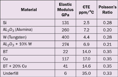
The material properties of the silicon, the substrate dielectrics and metals, and the underfill are provided in Table 1. Furthermore, the effective mechanical properties of the composite substrate structures are included, as calculated using the following formula:
 |
where P represents the property of interest: the CTE, elastic modulus, or Poisson’s ratio. Pi is the value of the property and hi is the thickness for layer i of a laminate composite having N layers. PEFF is the effective value of this property, which represents the mechanical behavior of the composite as a whole and is, in effect, a volume-weighted average of this property based on the individual values for each of the component materials. This approximation is justified by the fact that the metal in a substrate is usually fairly evenly distributed over its thickness.
Note that the effective value of the elastic modulus for the BT + Cu laminate substrate is much larger than that of the original BT material whereas that for the Al2O3 + W substrate is relatively close to that of the Al2O3. This is due to the much greater disparity in the elastic moduli for BT and Cu than for Al2O3 and W.
A commercial Finite Element Analysis (FEA) software tool was used to calculate warpage for both configurations [2]. Furthermore, a relatively simple analytical approach developed for the analysis of a two-layer structure (configuration 1 only) is examined and its accuracy calculated with respect to the FEA solutions [3].
FEA Solution
A solid model was created for each of the two configurations described above. In each, the Si chip was assigned a constant width of 15 mm. Separate simulations were run with the substrate width equal to 15 mm and then to 30 mm, in order to study the effect of the substrate width on the bending of the chip. Constant values of thickness were applied to the chip (0.5 mm) and substrate (1.0 mm) in all simulations. In configuration 2, the underfill thickness was assumed to be 0.1 mm. Linear elastic properties corresponding to those in Table 1 were assumed. A stress -free temperature of 170�C was assumed, along with a final temperature of 21�C. Temperature of 170�C corresponds to the glass transition temperature (TG) of the underfill.
 |
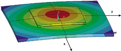
Figure 1. FEA model of die bonded to a substrate with an intervening underfill layer showing the effect of differential thermal strain. Contours indicating constant z-axis strain are superimposed on the solid model. The z-axis strain is magnified to better illustrate the spherical curvature of the surfaces.
The results are displayed in Figures 1 and 2. Fig. 1 depicts a typical contour map of z-axis strain or ∆z across the chip and substrate superimposed on the solid model. One observes a circular symmetry in the contour plot and that the chip curvature is that of a spherical surface.
 |
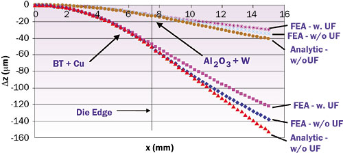
Figure 2. Plot of z-axis strain at mid-plane of substrate versus position along x axis as calculated using both FEA and analytical calculation methods for the two package configurations studied (with and without underfill) and both substrate types.
Figure 2 plots the values of ∆z versus x at the mid-plane of the substrate extracted from the finite element model for both configurations with both substrate materials. It is obvious that there is much more substrate warpage with the BT substrate than with the alumina one. This is due to the much greater CTE mismatch with Si (2.5 ppm/�C) for the BT substrate (14.6 ppm/�C) than for the alumina substrate (6.9 ppm/�C). One notes that for a given substrate, within the die footprint, its warpage follows a constant radius, nearly irrespective of the size of the substrate and the presence of the underfill. Beyond the die footprint, the configurations with an underfill show less warpage than those without it. This is clearly due to the lower modulus of the underfill compared with that of the die and the substrate, enabling it to reduce the mechanical coupling between these two components. Furthermore, beyond the die, the substrate is curved slightly upward
Analytical Calculation
The following expression can be used to calculate the radius of curvature for either the die or the substrate for the 2-layer configuration, with the substrate width equal to the die width [3].
 |
where the subscripts 1 and 2 refer to the lower and upper plates, respectively; R is the radius of curvature of the mid-plane of the upper plate; h = h2/h1 is the ratio of the thickness of the lower plate to that of the upper plate; m = M2/M1 is the ratio of the biaxial modulus of the lower plate (M2 = E2/(1- v2)) to that of the upper plate (M1 = E1/(1- v1)), where v1 and v2 are Poisson’s ratio for the two plates; and εm = (T-T0)(CTE1– CTE2) is the thermal mismatch strain between the two plates. In this simplified situation, Eqn. 2 accounts for the tradeoffs between the differing material properties, layer thicknesses, and ∆T in determining R.
∆z as a function of x is calculated using
where R is obtained from Equation 2.
The following expression for ∆z beyond the die footprint represents the tangent to the constant R curve at the edge of the die. It is not based explicitly on any physics, but merely this author’s observation that this would represent a reasonable approximation of the ∆z behavior beyond the die footprint demonstrated in Figure 2.
If x0 is defined as DieWidth/2 and ∆z0 is the value of ∆z at x0, then
 |
The profile for the substrate based on Equations 3 and 4 is plotted in Figure 2 along with the FEA results. To the eye, the agreement between the analytical and the FEA results within the die footprint is quite good.
Beyond the die, the straight-line profile generated by Equation 4, traces out larger values of ∆z than those predicted by the FEA calculations and is in reasonable agreement with the FEA results for the 2-layer configuration with which it shares the assumption of no underfill being present.
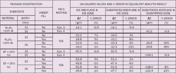
Table 2. Package Contruction and Results
 |
Table 2 provides the output of both methods in calculating the value of ∆z at the mid-plane of the die at the die edge and of the mid-plane of the substrate at both the die and the substrate edges. Furthermore, the table quantifies the error in the prediction of the analytical calculation (assuming no underfill) compared with that of the FEA simulations with and without underfill.
In summary, Equation 3 does a fine job of predicting the die warpage irrespective of the presence of underfill and the size of the substrate (error < 7%). The ability of Equation 3 to predict the warpage of the substrate depends on the particular assumptions made regarding the substrate size and presence of underfill. At the die edge, in the worst case, the error was �15%. At the edge of the 30 mm substrate, the worst case error is �39%. The largest errors in predicting the substrate warpage were associated with the alumina substrate and with the presence of underfill. The synergy of the large modulus of the alumina with the small modulus of the underfill led to less warpage of the alumina compared to that predicted by Equations 3 and 4.
Discussion
The analytical method just described can be used to predict die and substrate warpage under conditions beyond those assumed in their derivation with reasonable accuracy However, this is not sufficient to predict the occurrence of a failure mechanism even for the simple die/underfill/substrate stackup studied here. This is even more true for more complex package configurations in which a lid is bonded to the die and to the substrate or the substrate is attached to a printed circuit board by a matrix of solder balls.
However, it is possible to use a calculated value of chip warpage as a figure of merit. In general, the greater the warpage in the chip/underfill/substrate as an isolated assembly, the more likely that there will be die cracking or, in the more complex package configurations, a failure of an adhesive interface or a solder ball. In the event of such a failure the methodology explored here provides a method of determining the impact on the warpage of changing the physical parameters at the disposal of the packaging engineer: the thickness of the chip and the thickness, modulus, and CTE of the substrate.
References
- Guenin, B., “Thermal Strain in Semiconductor Packages, Part I,” ElectronicsCooling, Vol. 13, No. 1, 2007, pp 9-11.
- ANSYS, Ver. 10.0.
- Guo, Y., and Zhao, J.-H., “A Practical Die Stress Model and Its Applications in Flip-Chip Packages,” Proceedings of the Seventh Intersociety Conference on Thermal and Thermomechanical Phenomena in Electronic Systems, ITherm, 2000, pp. 393�399.


