Introduction
Predicting gallium arsenide (GaAs) semiconductor temperature is imperative since it affects the performance and reliability of the chip and the design as a whole. In many circumstances, the thermal engineer will be asked to provide expeditious and accurate answers to trade studies regarding various FET layouts and geometry, metallization schemes, and conduction paths from the chip down to the heat sink at multiple pulse widths, duty cycles, and power dissipations. The interaction of these parameters affects the thermal performance of a design and necessitates that the engineer have a fundamental understanding of material properties, steady state, and transient responses of each configuration [1].
Despite a full grasp of the above factors, the engineer must also employ tactics that overcome computer processing limitations and the fact that the geometry scale to be thermally resolved at the FET, compared to stackup layers towards the heat sink, can vary by as much as five orders of magnitude. Capturing all these effects in a temperature prediction can be a daunting task. This work discusses a modeling technique and scheme to predict the junction temperature of a GaAs chip efficiently and accurately by means of commercial finite difference thermal modeling software [2].
Problem Description
On a GaAs chip, heat is generated at discrete locations called gates or fingers. The heating is due to the electrical resistance faced by current as it traverses from source to drain circuitry, with the heat generation slightly favoring the drain side. Figure 1 depicts heat generation within a GaAs semiconductor. For the purposes of the modeling results presented, heat generation is assumed to be directly under the gate metal.
Groups of source, drain, and gate metal that are aligned in parallel and tied together electrically are called FETs and groups of FETs are called cells [3]. Although finger length and pitch are shown in Figure 1, finger width is into the page. Typically, a GaAs chip consists of multiple cells positioned on top of the GaAs chip to achieve a desired electrical output. In a typical stackup, the heat conduction path from the chip to the heat sink is as follows: chip → solder → tab → epoxy → metal baseplate → thermal interface material (TIM) → heat sink.
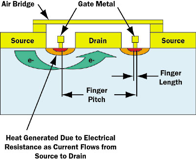 |
Figure 1. Heat generation within a GaAs chip.
Modeling Techniques
The first step to perform a thermal analysis on a chip with the stackup previously mentioned is to generate a cell-level model whereby the heat generated by the gates is uniformly distributed over the cell area. The problem at hand is a fully 3-D conduction heat transfer problem and the mesh generation needs to take this into consideration. A good practice is to use a high mesh density close to the heat generation sources and relax the mesh further from them. This is shown in Figure 2.
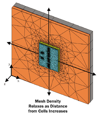 |
Figure 2. 3-D model of a cell-level chip stackup model.
The intent here is to provide an efficient model that resolves temperature gradients below the chip during a pulsed condition and to determine how far the peak power propagates into the stackup during the pulsed condition. The general solution technique is to first solve the model steady state with average power applied uniformly over the cells. By running the pulsed model from the initial conditions established for the steady state model with average power, the peak temperature and transient gradients are established within three periods. The temperature gradients established from the solution of this model remove initial transients that would be seen if the pulsed model was started with the stackup at a uniform temperature, thereby reducing computing time. Temperature gradients through the GaAs, especially near the gates, are not intended to be resolved with this model.
Depending on the length of the pulse width and heat storage capabilities of the stackup materials, temperature gradients at the top of the stackup will be affected by peak power while temperature gradients toward the bottom of the stackup will be affected only by average power. Average power is determined by multiplying the duty cycle by the peak power. A long pulse width will increase the temperature gradient in the top layers of the stackup as these layers “see” peak power for a longer time compared to a short pulse. A large duty cycle will increase the temperature gradient in layers that “see” only average power. For the purposes of this article, a pulse width less than 1ms is considered a short pulse and a pulse width greater than 1ms is considered a long pulse. Figure 3 shows an example of pulse propagation into a typical stackup.
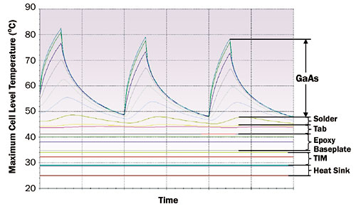 |
Figure 3. Cell-level temperature vs. time for a typical stackup.
In the case of Figure 3, the pulse propagates into the solder, which results in the chip and solder being affected by peak power. The tab, epoxy, baseplate, TIM, and heat sink are governed by average power dissipation. Figure 3 is typical of the short pulse width condition (< 1ms pulse width) while long pulse widths typically yield peak power down to the epoxy level.
Once the transient analysis of the cell-level model has been completed, resolving the temperature gradient through the GaAs must be performed. The cells are composed of FETs that contain multiple fingers. One cell may contain less than 10 fingers or could contain more than 100 fingers. Since the thermal engineer’s goal is to determine peak junction temperature at the end of a pulse, modeling only one fourth of a finger provides an expeditious and conservative means to obtain it [4]. This method employs mirror symmetry about the axis along the pitch of the fingers, and the fact that, for fingers in the middle of a cell, heat transfer only occurs through the GaAs and along the width of the finger. This conduction path is a consequence of the fact that there are adiabatic walls half the distance of the pitch on either side of the finger width. The extension of the resultant one quarter model along the finger width depends on how close another cell is to the one being modeled or if the model becomes limited by the chip periphery. Figure 4 shows an example of a finger-level model.
Typically, temperature gradients along the finger width (y-direction) are negligible compared to those in the first few microns underneath the finger. Therefore, the node-to-node distance along the width of the finger (y direction) versus directly below the finger (z-direction) can be 2-3 orders of magnitude greater. Although the model shown in Figure 4 contains source metallization, the drain metallization, air bridges, and vias through the GaAs are not included. Adding these features can double or triple the model construction time and represent a secondary heat path that can reduce the temperature rise in the GaAs by 10-20% [4]. Their omission will lead to conservative predictions of junction temperature and expedite the generation of results, especially when numerous analyses are required.
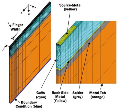 |
Figure 4. 3-D finger-level model.
The boundary condition for the finger model shown in Figure 4 depends on how far the pulse width propagates into the stackup. Using the example shown in Figure 3, a boundary condition of 41�C would be applied to the bottom of the metal tab in the finger model shown in Figure 4. Using the boundary condition, pulse width, duty cycle, and power dissipation information, a finger-level transient analysis can be performed to obtain the peak junction temperature of the chip with the finger level geometry resolved. An example of a finger level transient is shown in Figure 5.
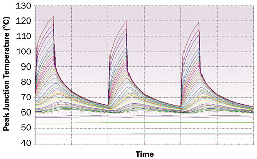 |
Figure 5. Finger-level transient.
If a finger level analysis of a long pulse is required, especially a case where the pulse width far exceeds 1ms, a steady state analysis using peak power will yield accurate results. Pulse widths beyond 1ms are typically long enough to allow the GaAs to reach steady state (> 3 time constants). Therefore, a finger model including only the GaAs and the solder layer with the boundary condition applied at the bottom of the solder is sufficient to predict the peak junction temperature. If the pulse width is approximately 1ms, the thermal time constant can be calculated by multiplying the thermal resistance by the specific heat of the GaAs and the solder to confirm if the steady state finger level analysis is valid [5].
Although the modeling techniques mentioned previously assume the validity of Fourier’s Law at the cell and finger level, classical heat transport theory begins to breakdown at a length of 0.3 microns. If more detail is desired at the finger level less than 0.3 microns, recent work has provided a means to quantify heat transfer in this regime [6].
Conclusions
Thermal modeling of GaAs semiconductors using the aforementioned techniques provides a conservative and expeditious approach to generating multiple results, which can be used by both mechanical and electrical designers in evaluating design and product performance. If increased accuracy is desired, such as capturing the effects of all the chip metallization and vias, more foresight in model construction must be employed to keep the minimum time step of the thermal model at a reasonable value for the pulse width being analyzed. Although this article’s primary focus is predicting chip junction temperature using numerical modeling approaches, analytical methods based on classical heat transport theory still provide valuable insight and comparable accuracy into transient thermal phenomena within a chip.
References
- Wilson, J., “Thermal Issues in GaAs Analog RF Devices,” ElectronicsCooling, February 2002.
- ANSYS Thermal Analysis Software, Version 8.2.11.
- DeLorenzo et al., “GaAs FET Principles and Technology,” Artech House, 1982.
- Harper, C., “Passive Electronic Component Handbook,” Second Edition, Chapter 9 – Electronic Device Cooling, McGraw-Hill, 1997.
- Incropera, F., De Witt, D., “Fundamental Heat and Mass Transfer,” Fifth Edition, Wiley, 2006.
- Ashegui, M., Liu, W., “Microscale Heat Transfer,” ElectronicsCooling, February 2007.


