The primary approach to maintaining the aggressive progress in the microelectronics industry has been to increase the density of elementary transistors and to reduce the size of their active areas. As a result, the removal of heat generated by various internal system components has become a major design challenge, further complicated by the lack of knowledge of the temperature behavior of critical features. Thus, there is an increased demand for methods that can determine temperature distributions at the submicron level.
Clearly, in order to measure the active junctions of modern devices, which are frequently powered in a pulsed mode, a method needs to have superior spatial and temporal resolutions. The use of contact methods introduces the added difficulties of having to access features of a submicron device with an external probe, or, in the case of embedded features, of having to fabricate measurement probes into the device, and then having to isolate and exclude the influence of the probes themselves.
Among the various optical approaches, the thermo-reflectance method possesses important advantages and, to date, is one of only a couple of methods that have been successfully used to perform temperature mappings at the submicron level. Thermo-reflectance thermography (TRTG) is a cost-effective, non-contact and non-destructive optical approach for probing steady-state and transient surface temperature, providing accurate results for submicron features of microelectronic devices with excellent spatial, temporal, and thermal resolutions.
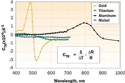
Thermo-reflectance microscopy is based on the principle that a change in the temperature of a given material produces a small change in the reflectivity of that material’s surface. Thus, to measure the increase (or decrease) in the temperature of a sample, ΔT, one needs to measure the relative change in the reflectivity of the sample, ΔR/R, and know the thermoreflectance coefficient that relates them, CTR. The latter is a function of the material under test, the wavelength of the probing light, and even the composition of the sample if the sample is multi-layered with transparent or semi-transparent materials present in the path of the probing light.
 |
Figure 1. Examples of measured CTR values for selected materials.
The most challenging issue for thermoreflectance measurements is the small value of the thermoreflectance coefficient, typically on the order of 10-3 to 10-5 per Kelvin for most electronic materials. Naturally, obtaining a temperature distribution with a good level of accuracy requires that CTR be sufficiently high in order to achieve an appropriate signal-to-noise ratio. Fortunately, the dependence of CTR on light wavelength provides an opportunity to tune the probing light to the material under test. However, since the overall measurement uncertainty is dominated by the uncertainty in the value of CTR, it becomes imperative to measure CTR carefully and preferably in situ. Figure 1 provides examples of the variation of CTR for different materials over all visible and near -infrared light wavelengths.
Once the calibration step is completed by determining CTR for the materials of interest, measuring their temperature field resulting from internal heating requires obtaining the rate of change of reflectivity on their surface. The reflectivity change can be detected either by a photodetector [1] or by a CCD camera [2]. The light source for a photodetector-based system must be a laser in order to measure a single point, while an LED or a variable wavelength light source can be used to illuminate a surface area when measuring with a CCD camera. The advantages of the latter approach are that it is simpler to use, is easier to vary the wavelength of the probing light (to maximize the CTR coefficient), and has excellent spatial resolution (as low as 200 nm). The main advantage of the laser -photodetector approach is its ability to measure fast transients, up to 500 MHz, which is more than sufficient to capture most transient thermal responses.
|
||||||||||
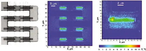
For a demonstration of the superior spatial resolution of the TRTG method, We have used the CCD approach to measure the surface temperature field of a MOSFET IC with eight fingers (Figure 2). The active region of the 1-mm gate consists of 300 � of SiGe on a Si substrate. The SiGe is covered by successive layers of 100 � gate oxide, 500 � poly-Si, and 1500 � SiO2. The temperature field measurement is made on the poly-Si surface through the SiO2 passivation layer with a 565 nm probing light.
For existing devices, the highly resolved and accurate 2D temperature fields obtained with the TRTG system provide the ability to detect hot spots, diagnose performance, and assess reliability. In the design and manufacturing of new devices, this new metrology tool has the potential to provide a rapid approach for analyzing the thermal behavior of complex stacked structures, to identify regions of excessive heat densities, and ultimately to contribute to improved thermal designs, better device reliability and shorter design cycle times.
References
The interested reader can find additional background information and references to important contributions of other research groups in the following publications:
- Burzo, M. G., Komarov, P. L., and Raad, P. E., “Non-Contact Transient Temperature Mapping of Active Electronic Devices Using the Thermoreflectance Method,” IEEE Transactions on Components and Packaging Technologies, Vol. 28, No. 4, 2005, pp. 637- 643.
- Komarov, P. L., Burzo, M. G., and Raad, P. E., “CCD Thermoreflectance Thermography System: Methodology and Experimental Validation,” THERMINIC 12, Nice, France, 2006.


