Introduction
The role of thermal interface materials (TIM) to augment heat flow in electronics has been well-documented [1-4]: Higher thermal conductivity (k) and thinner bondlines proportionally reduce the interface thermal resistance (RTH). Today’s high-performance TIMs contain micro- and nanometer-sized particles to increase the effective TIM thermal conductivity (keff,TIM) compared to the bulk fluid, e.g., from 0.15-0.20 W/mK silicone oil to a keff,TIM > 5 W/mK silicone-based TIM. The benefit in increased keff,TIM can be offset at high fill factors when the fluid properties prevent formation of a sufficiently thin bondline. Further TIM improvements, therefore, rely on the formation of thin bondlines at reasonable assembly pressures in highly-filled compositions. We have shown that paste interfaces can be formed with lower pressure and thinner bondlines by hierarchically nested channel (HNC) structures [5-7]. The reduction in thermal resistance and assembly loads is attractive for automotive, power electronics, optical, RF, and microprocessor packaging; enabling higher-power operation at lower junction temperature.
Design Considerations
The channels relieve pressure during the assembly squeeze, offsetting the effective non-Newtonian viscosity increase due to particle loading. The assembly dynamics are described by Stefan (squeeze) flow with a crucial modification: The square interface in electronics packages causes the fluid flow to bifurcate along the diagonal because the flow path to the edge of the interface is shorter (Figure 1). The bifurcation also causes local variation in particle fill factor that leads to spatial keff,TIM variations or electrical resistivity variations for electrically-conductive formulations as the particles may be suspended at the bifurcation lines.
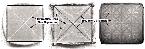 |
Figure 1. Flow bifurcations due to TIM squeezing on flat (left), HNC1 (middle), and HNC2 (right) interfaces of an 18 x 18mm2 chip. The flat and HNC1 images are optical, the HNC2 image is an acoustic scan.
Channel Hierarchy
The diagonal (“HNC1”) channels reduce the pressure, redistribute the flow field, and create new TIM bifurcations corresponding to flow being distributed either to the edges of the chip or the channels (middle picture, Figure 1). Additional channels (“HNC2”) further sub-divide the flow, but the cross section of these second-level channels can be smaller because the maximum local pressure is lower. This leads to the hierarchical nature of the technology � additional channels carry proportionally less TIM material and can have smaller cross sections. Bondline thickness (BLT) reduction due to the channels must offset the removal of highly-conductive solid material from the system. The hierarchical design ensures that the impact of removing solid is proportionately less for each additional channel “level”, corresponding to the proportionately lower impact of additional HNC levels on reducing BLT and assembly pressure. Nevertheless, coupling the thermal and flow impact of HNC leads to an optimum point, at which further HNC levels begin to increase rather than decrease the thermal resistance of the interface [7].
Channel Geometry
There are four characteristic length dimensions in the HNC system: the particle size distribution, the channel dimension, the bondline thickness, and the interface size. The filled TIM can be captured as a Bingham fluid with a yield strength that increases with particle loading and causes the effective viscosity of the TIM to increase with decreasing shear rate.
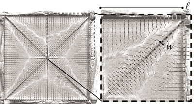
Previous work [8] using three-dimensional computational fluid dynamics (CFD) compiled all characteristic lengths into one model coupled to a compact thermal system to prescribe a simple design rule for HNC1. We found that thermal interface resistance is reduced most when the width ( w, Figure 2) of the square channels measure 3.4% of the total length of the interface (2�l, Figure 2). This corresponds to 600 �m HNC1 channels in a typical 18 x 18mm2 microprocessor-to-lid interface or 1.7 mm channels in a 50 x 50mm2 lid-to-cooler arrangement. Extending the analysis to further channel hierarchy levels is more complicated, but follows the same basic rule.
Figure 2. Flow vectors from numerical simulation mapped onto optical image of paste bifurcation, denoting the relevant geometries for the HNC1 design rule.
Results and Discussion
We have characterized over 20 materials with HNC and found > 20% BLT reduction for up to three HNC levels (HNC3). The technology was first developed as a “TIM1” (silicon chip to lid) solution, but current work suggests even greater benefit on larger interfaces, for example, power electronics modules. On such 100 x larger areas, HNC can improve thermal performance without the effort and expense of qualifying and implementing newer paste formulations.
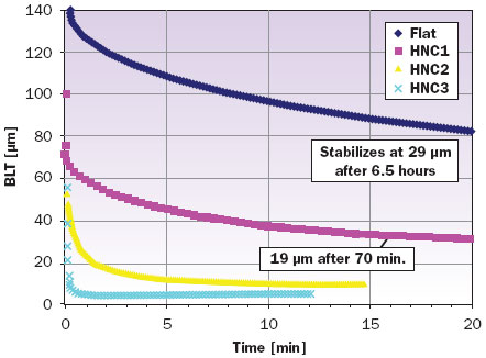
Figure 3. Temporal bondline assembly profile for Wacker P12 silicone-based TIM common in power electronics applications. The 14 x 20 cm interface was assembled with 2 bar pressure.
The temporal assembly profile of a typical power electronics module and paste follows the trend observed in TIM1 measurements [7]. Figure 3 shows:
1) The final BLT significantly reduces for increasing levels of HNC;
2) The squeeze time, i.e. the time to reach final BLT, is reduced with higher levels of HNC; and
3) The absolute reduction of final BLT and squeeze time decreases with additional levels of HNC.
The thinner bondlines in HNC1-HNC3 proportionally reduce RTH,interface but even more dramatic is the reduced assembly time (Table 1). This can be significant for module burn-in procedures and may allow the bondline formation to couple to the curing time for adhesive TIM applications.
Table 1. Summary of HNC effects on BLT for selected materials on 280 cm2 test stand
All reported data taken at 25�C; higher temperature (60�C) assembly reduced final BLT and squeeze time by 5-60%, depending on TIM formulation. Squeeze time defined by time required to reach 102% of final BLT.
Machining tolerances and mechanical considerations often require BLT > 50 �m in large-area modules. In these cases, HNC can be used to implement higher-keff,TIM pastes that could not be squeezed sufficiently thin otherwise. Although it may not be possible to eliminate 80% of RTH,interface by thinning a 1-W/mK, 100-�m paste to 20 �m, replacing it with a 5-W/mK formulation that can be thinned to 100 �m by means of HNC attains the same RTH,interface reduction within mechanical specifications. Even when thin bondlines can be tolerated, thermal contact resistance sets the lower bound where further bondline thinning does not improve thermal performance.
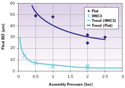
Assembly pressure is a third factor that can be addressed with HNC (Figure 4). While the final BLT is dependent on pressure for any non-Newtonian formulation (a Newtonian fluid would eventually reach zero thickness), HNC decouples this relationship. For all pressures, HNC results in lower BLT than a flat interface and the minimal BLT is reached for lower pressure. From Figure 4 it is evident that beyond one bar, additional assembly pressure yields little additional BLT reduction. Lower assembly pressures may then ease the mechanical strength requirements of the modules and tools, possibly yielding cost reductions.
Figure 4. Effect of assembly pressure on final BLT for flat and HNC3
power modules using the same TIM as in Figure 3.
Summary and Outlook
HNC improves thermal interfaces by enabling thinner bondlines with higher-performance pastes at lower assembly pressure. The effects are most dramatic in large-area applications, where a 90% or greater reduction in squeeze time can reduce assembly time and burn-in while enabling shorter cure times for adhesive TIM applications.
Practical Considerations
Some TIM formulations are not well-suited for HNC. Low-viscosity pastes with large particles prematurely stop the squeezing process. Stencil or screen printing the TIM tends to remove excess paste before assembly that the channels would otherwise handle during the squeeze, reducing the HNC benefit for current module geometries. Finally, small (TIM1) interfaces generally achieve smaller percent improvement from HNC with existing pastes. The challenge may rest in cooperation between paste and component vendors to formulate appropriate paste-HNC combinations that can reach the performance of high-cost solutions [5].
Although HNC is a low-cost solution, it is not a no-cost solution. We estimate less than 10% added cost to lids or coolers for suitable large-volume manufacturing processes. Laser cutting, chemical etching, and electrical discharge machining (EDM) are possible for high precision, high margin applications; however, we are focused on stamping, machining, extrusion, and injection molding. The cost may be at least partially recovered in the ancillary cost benefits of HNC; for example, by reducing a module’s mechanical strength specification.
Ongoing Work
One particularly attractive subject is the effect of HNC on the reliability of the thermal interface. The channel patterns in the surface absorb air voids trapped during bondline formation, prevent paste “bleeding” and nonuniformities that develop over time (Figure 5), and reduce the “pump out” seen after thermal cycling. Increased reliability could extend component lifetime and maintenance intervals, yielding further cost reduction.
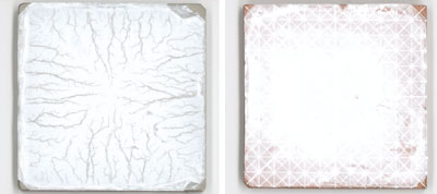 |
Figure 5. HNC effect on phase separation of silicon (PDMS)-based TIM with approximately 65% ZnO volume fill. Left: flat TIM2 lid with well defined bleeding traces along the squeeze flow path; right: same lid size, but with HNC2 on the 48 x 48 mm interface.
Investigations are ongoing to identify the TIM composition and particle distributions that most affect HNC bondline formation to improve existing models and collaborate with component and paste vendors on commercialization. In addition, we are screening for further industries that may benefit from HNC. Electrically-conductive applications and solar concentrator photovoltaics (CPV) share many of the same high thermal and electrical performance requirements, and thus are interesting candidates.
Acknowledgements
The authors would like thank Ryan Linderman, Urs Kloter, Hugo Rothuizen and Thomas Brunschwiler for previous work on the HNC technology, and recognize the support of European Commission under the Nanopack project of the Seventh Framework Programme (2007-2013).
References
- Gwinn, J., Webb, R., “Performance and Testing of Thermal Interface Materials,” Microelectronics Journal 34 (3), 2003., pp. 215-222.
- Singhal, V., Siegmund, T., Garimella, S., “Optimization of Thermal Interface Materials for Electronics Cooling Applications,” IEEE Transactions on Components and Packaging Technologies, 27 (2), 2004, pp. 244-252.
- Prasher, R., “Thermal Interface Materials: Historical Perspective, Status, and Future Directions,” Proceedings of the IEEE, 94(8), 2006, pp. 1571-1586.
- Yovanovich, M.,”Four Decades of Research on Thermal Contact, Gap, and Joint Resistance in Microelectronics,” IEEE Transactions on Components and Packaging Technologies, 28 (2), 2005, pp.182-206.
- Linderman, R., Brunschwiler, T., Smith, B., and Michel, B., “High-Performance Thermal Interface Technology Overview,” Proc. 13th Conf. on Thermal Investigations of ICs and Systems “THERMINIC 2007,” Budapest, Hungary, September 2007, B. Courtois et al. (Eds.) (EDA Publishing/Therminic 2007, Budapest, Hungary), pp. 129-134.
- Brunschwiler, T., Kloter, U., Linderman, R., Rothuizen, H. and Michel, B., “Hierarchically Nested Channels for Fast Squeezing Interfaces with Reduced Thermal Resistance,” IEEE Transactions on Components and Packaging Technologies, 30 (2), 2007, pp.226-234.
- Linderman, R., Brunschwiler, T., Kloter, U., Toy, H., and Michel, B., “Hierarchically Nested Surface Channels for Reduced Particle Stacking and Low-Resistance Thermal Interfaces,” Proc. 23rd Annual IEEE Semiconductor Thermal Measurement, Modeling, and Management Symp. “Semi-Therm 2007”, San Jose, CA (IEEE, 2007), pp. 87-94.
- Smith, B., Rothuizen, H., Linderman, R., Brunschwiler, T., Michel, B., “Design of Thermal Interfaces with Embedded Microchannels to Control Bond Line Formation,” Proc. 11th Intersociety Conf. on Thermal and Thermomechanical Phenomena in Electronic Systems 2008 “ITHERM 2008,” Orlando, FL, May 2008 (IEEE, 2008), pp. 410-418.

