Introduction
As consumers of electronics we have become spoiled. We not only expect our electronic devices to get smaller, faster, more functional, cheaper, more interconnected, and more reliable, we actually demand it. It would not be a pretty picture either for the consumer or the electronics industry if suddenly the design of our electronic gadgets became static. At this point, shopping for a new cell phone would be as exciting as looking for a new toaster � and it would probably be as frequent.
Of course, we all attribute this trajectory of constant progress in our electronic hardware to Moore’s Law — the continued miniaturization of the electronic circuitry in ICs.
In this article, we explore the greater implications of Moore’s Law on IC performance, the increasing challenges the IC fabrication industry is facing in maintaining the pace set by Moore’s Law, the promise of 3D packaging in making up for any shortfall in IC performance, and the thermal challenges faced by 3D packaging.
Moore’s Law Scaling
The formulation of what we call Moore’s Law began in an article written in 1965 by Gordon Moore, one of the founders of Intel [1]. In it he notes that, at that moment in time, the number of transistors on an IC was doubling every year. He saw no reason why this shouldn’t continue and predicted that this trend would continue at least through 1975, when, according to his trend line, ICs should have 64,000 transistors. This was a fairly bold prediction for its time, since at that moment production ICs only had about 64 transistors.
This process of reducing the area of a transistor by 50% is accomplished by shrinking its linear dimension by roughly 30%. Equivalently,
 |
where LTRANS is the width of a transistor cell and ATRANS is its area.
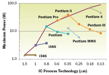
This dimensional scaling behavior has a beneficial effect on the power dissipated by the transistor. This behavior is captured by the trend lines in the graph in Figure 1, that relate the power dissipated by different generations of Intel processors, in the late 1980’s and 1990’s, and the technology nodes used in making them [2]. A given generation or node of IC fabrication process technology is identified by a characteristic length equal to one-half of the pitch of the minimum-sized metal lines that can be fabricated with that technology.
Figure 1. Impact of IC process technology on processor power, at introduction, and as processor is ported to subsequent generation technologies.
The fabrication technologies span the range between 1.5 �m and 0.13 �m. The characteristic lengths for successive technology generations follow the scaling behavior of Equation 1. In that era, the transition from one technology node to the next took three years and was accompanied by the doubling of the clock frequency.
As each processor was introduced, its power was higher than that of its predecessor at the time of its own introduction. This is captured in the usual processor power trendline showing a continual increase over time. However, each of these new processors was typically 25% larger in area than its predecessor, and had 75% more transistors, due to the 50% shrinkage in the area of a single transistor. These factors mask the true effect of Moore’s Law on power scaling. When a particular Pentium processor, with a constant number of transistors, was fabricated in successive technology generations, it manifested a power scaling factor of 0.71, even though the frequency doubled with each generation. This was accomplished by reducing the core voltage by a factor of 0.71, made possible by the reduced capacitance of the smaller transistors. In contrast, the i386 and i486 processors were designed to use a constant core voltage and did not show a power reduction as the fabrication technology moved on to the next generation.
Present and Future of Moore’s Law
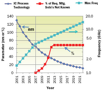
The International Technology Roadmap of Semiconductors (ITRS) maintains several committees which track the status of critical technologies for the design, fabrication, test and packaging of ICs. Figure 2 captures some of the implications of their latest full report, published in 2007 [3]. It shows the progression in CMOS fabrication technologies for the years 2001 � 2022. They range from 130 nm to 11 nm, with a 2-year Moore’s Law cycle in 2001-2008 and a 3-year cycle thereafter. This increased cycle length is a reflection of the expectation of the ITRS that the industry will be facing greater challenges moving forward.
Figure 2. Processor trends as reported by ITRS in 2007: IC process technology and maximum clock frequency. Red symbols indicate the percentage of the set of lithographic requirements identified by the ITRS for which there were no known manufacturable solutions.
The ITRS tracks a total of 19 lithography requirements in terms of the availability of proven manufacturing solutions. The current technology (2007 -2010) is 65 nm. This value would have to be reduced to 45 nm by 2010. The red symbols in Figure 2 indicate the percentage of these requirements for which there are no manufacturable solutions known at this time. This percentage increases rapidly from 0% in 2007 to 21% by 2010. This number is predicted to plateau at 68% by 2013, when the 32 nm technology would need to be available to maintain the targeted Moore’s Law pace.
Finally, the clock frequency trend line shows a break at 2007. Up to that point, the frequency was increasing by 21% per year. After 2007, the ITRS prediction is that frequency will increase by only 8% per year.
There are other challenges as well. Shrinking transistor sizes lead to greater statistical variations in device dimensions and chemistry and subsequently to their electrical characteristics and to increased leakage currents.
The ITRS analysis does not eliminate the possibility of technological breakthroughs to enable the prolongation of Moore’s Law scaling over the next decade. However, it does indicate that things will probably be very difficult.
3D Packaging Solutions
The industry still has means available to it to provide the market with products offering the same sorts of improvements made possible in the past by Moore’s Law. These approaches can help to maintain the system-level performance improvements required by the end user, but without the need to shrink the transistor size. This would be accomplished by integrating more functions currently performed by separate ICs and other components into a single package through the adoption of 3D packaging structures.
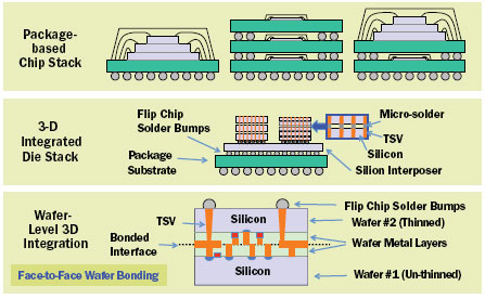
Figure 3 depicts a number of 3D package solutions. They are categorized into three general classes: package-based chip stack, 3-D integrated die stack, and wafer-level 3-D integrated chip, and are discussed below [4, 5].
Package-based Chip Stack
Package-based chip stacking technology is currently used mainly for stacked memory chips. The 3rd dimension in the electrical interconnect is traversed either by bond wires or package substrates interleaved by solder balls or a combination of both. These packages are being used in mobile applications, such as cell phones, where compactness comes at a premium. The wirebonded packages employ chips thinned to as little as 50 �m in stacks up to 5 high [6].
Package-on-Package (PoP) designs do not achieve the compactness of stacked chips. However, the individual packages can be electrically tested before stacking and offer better signal integrity than stacked chips, with their long bond wires.
The manufacture of both package types involves standard packaging technology with typical wiring and I/O pitch and interconnect densities.
Integrated 3D Chip Stack
3D integrated die stacks are assembled with aspects of both standard and wafer-level packaging. Through-silicon-vias (TSVs) are used to provide a vertical electrical interconnection within each chip. The TSVs are made in each thinned chip by drilling holes using either laser ablation or deep reactive ion etching (DRIE) [5]. The sides of the holes are then coated with an insulator, followed by a thin conductor onto which the via metal is electrodeposited. The electrical interconnection between adjacent chips in the stack can be achieved by conventional C4 bump or low-profile solder or thermocompression bonds to reduce the interchip spacing [7]. Since TSVs can be fabricated at pitches of tens of microns, interconnect densities can be achieved that are more than three orders of magnitude higher than that of the package-based stacking technology.
This technology can accommodate stacks with larger numbers of chips within a smaller form factor and with better signal integrity than is possible with wire-bonded stacked chips. It is now nearing commercialization. Various examples of packages using this technology are shown in Figure 3.
 |
Figure 3. Major types of 3D packages along with specific examples.
Wafer-level 3D Integrated Chip
3D wafer-level integration represents the ultimate stage of integration in 3D packaging. It incorporates many of the standard CMOS fabrication processes with an elaborate series of BEOL (back end of line) techniques to construct a 3D wafer, layer by layer. It involves sequentially bonding thinned wafers together. After bonding each wafer, it is electrically connected to the preceding one using TSVs.
The end result is a multilayer wafer with circuits that are interconnected with lines fabricated at the full resolution available in CMOS technology. In a 45 nm technology it would be possible to use CMOS wafers thinned to only 4 �m, which would allow TSVs to be fabricated at a pitch as small as 400 nm. The electrical interconnection between layers would be accomplished by copper diffusion bonding. Options for interwafer bonding involve either organic (BCB [benzocyclobutene]) or inorganic (SiO2) materials.
The process technologies needed for commercializing 3D wafer fabrication are still under development. 3D wafers are not expected to impact the market until the next decade [7].
3D wafer-level integration offers the greatest possibility for maintaining and even exceeding the rate of miniaturization provided by Moore’s Law when the volumetric efficiency at the system level is considered. Furthermore, it offers the promise of significant cost reductions at the system level, since interconnections between hundreds of chips would be made in parallel at the wafer level rather than through the current infrastructure of numerous packages, printed wiring boards, and solder joints. Finally, it lends itself to the integration of ICs representing heterogeneous technologies (e.g., CMOS + image sensors or optical devices or RF amplifiers). Hence, it is expected to offer significant opportunities for extreme device miniaturization for handheld applications.
Thermal Management of 3D Packages
In many current 3D packages, involving low-power flash memory, for example, the thermal management issues are trivial. However, in time, in order to maintain a Moore’s Law rate of performance scaling, it will be necessary to migrate to 3D packaging for all sorts of devices, including processors.
In side-by-side multi-chip packages, the area available for heat transport to the heat sink scales with the number of devices. Hence, there are no intrinsic barriers to cooling a large number of chips configured in this way. However, with 3D packages, the heat dissipated by all the layers of circuitry share a common thermal path. The thermal gradient suffers from the compound effects of aggregated power and a longer thermal path [8].
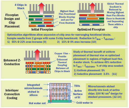
A number of methods have been described in the literature for dealing with the unique challenges in the thermal management of integrated 3D packages. They are briefly described in Figure 4 along with references for further reading [9-14].
Figure 4. Examples of solutions to the unique challenges in the thermal management of 3D packages.
Conclusions
Moore’s Law has for decades been the engine driving a significant portion of the technical progress made in the electronics industry. As the fabrication technology approaches 32 nm, the industry is facing significant challenges in maintaining its historical rate of performance growth. 3D packaging is currently providing the same sort of benefits at the system level as Moore’s Law has at the transistor level. Further developments in 3D wafer technology will be necessary to maintain a rate of technical progress required for the health of the electronics industry. 3D packaging brings with it significant thermal management challenges along with unique solutions when compared with traditional chip and packaging configurations.
References
- Moore, G. E., “Cramming More Components onto Integrated Circuits,” Electronics, Vol. 38, No. 8, 1965, pp. 114�117.
- Borkar, S., “Design challenges of technology scaling,” IEEE Micro, Vol. 19, No. 4, 1999, pp. 23�29.
- International Technology Roadmap for Semiconductors, 2007 Edition. Available for free download at http://www.itrs.net/Links/2007ITRS/Home2007.htm
- Lu, J-Q, Rose, K., and Vitkavage, S., “3D Integration: Why, What, Who, When?” Future Fab, No. 23, July, 2007, pp. 25-27.
- Knickerbocker, J., Andry, P., Dang, B., Horton, R., Interrante, M., Patel, C. S., Polastre, R., Sakuma, K., Sirdeshmukh, R., Sprogis, E., Sri-Jayantha, S., Stephens, A., Topol, A., Tsang, C. K., Webb, B. , and Wright, S., “Three-Dimensional Silicon Integration,” IBM J. Res. & Dev. Vol. 52 No. 6, November, 2008, pp. 553-569.
- Beyne, E., “The Rise of the 3rd Dimension for System Integration,” Proc., IEEE Int. Interconnect Technology Conference, 2005, pp. 1-5.
- Bernstein, K., Andry, P., Cann, J., Emma, P., Greenberg, D., Haensch, W., Ignatowski, M., Koester, S., Magerlein, J., Puri, R., and Young, A., “Interconnects in the Third Dimension: Design Challenges for 3D ICs,” Proc., Design Automation Conference, 2007, pp 562-567.
- Guenin, B., “Thermal Calculations for Multi-Chip Modules,” ElectronicsCooling, Vol. 8., No. 4, November, 2002.
- Cong, J., Wei, J., and Zhang, Y., “A Thermal-Driven Floorplanning Algorithm for 3D ICs,” in Proc., IEEE Int. Conf. on Computer-Aided Design, 2004, pp. 306-313.
- Wong, E., and Lim, S-K, “Whitespace Redistribution for Thermal Via Insertion in 3D Stacked ICs,” Proc., 25th Int. Conf. on Computer Design, 2007, pp 267-272.
- Goplen, B., and Sapatnekar, S., “Placement of Thermal Vias in 3-D ICs Using Various Thermal Objectives,” IEEE Trans. On Comp.-Aided Design of Integrated Circuits and Systems, Vol. 25, No. 4, 2006, pp. 692-709.
- King, C.R., Sekar, D., Bakir, M. S., Dang, B., Pikarsky, J., and Meindl, J. D., “3D Stacking of Chips with Electrical and Microfluidic I/O Interconnects ,” Proc., Electronic Components and Technology Conf., 2008, pp. 1-7.
- Yu, A., Khan, N., Archit, G., Pinjala, D., Toh, K-C, Kripesh, V., Yoon, S-W, and Lau, J. H., “Fabrication of Silicon Carriers with TSV Electrical Interconnections and Embedded Thermal Solutions for High Power 3-D Package,” Proc., Electronic Components and Technology Conf., 2008, pp. 24-28.
- Brunschwiler, T., Michel, B., Rothuizen, H., Kloter, U., Wunderle, B., Oppermann, H., and Reichl, H., “Forced Convective Interlayer Cooling in Vertically Integrated Packages,” Proc., iTherm Conf., 2008, pp. 1114 � 1125.


