Introduction
Significant increases in temperature are believed to contribute to losses in reliability and performance, and can present serious complications to thermal management. The net thermal effect depends on a combination of factors related to the feature size, power densities, and material properties. In semiconductor devices, higher heat flux densities can result from miniaturization (i.e., reduction in volume) and higher performance (i.e., increase in power), but either way the outcome is increased temperatures. The use of new materials in device fabrication introduces an uncertainty in the temperature rise that a device may experience. In effect, any new design of a device alters the compromise between performance, cost, functionality, and reliability of that device. In the case of micro-devices, a major reason behind a departure from a previously achieved compromise is a change in the device performance, which typically and unhelpfully ends up being a rise as opposed to a drop in temperature. Both the magnitude of this departure and the means to rectify it can be guided through thermal characterization of the device of interest. This article addresses the underlying challenges of thermal computations at submicron scales and presents selected useful solutions based on the authors’ work in thermal computational analysis.
Thermal Characterization
Thermal characterization can be physical (i.e., experimental) or mathematical. The authors have previously addressed in a technical brief [1] a promising experimental approach that is capable of non-invasively measuring device surface temperature fields with submicron resolution. The present article focuses on mathematical characterization.
The physics of heat transfer at the die level in microelectronic devices is primarily limited to conduction, with typically relatively negligible contributions of convection and radiation. In the continuum regime, the physics of heat conduction are described mathematically by the Fourier parabolic equation, expressing temperature as a function of time and three-dimensional space, and involving material density, specific heat, and thermal conductivity as parameters. A well-posed problem requires the imposition of appropriate initial and boundary conditions. For some microelectronic materials, the thermal conductivity can depend on temperature, rendering the governing equation nonlinear and thus more complicated to solve.
The mathematical analysis of heat transfer physics in a microelectronic device is typically performed in one of three primary solution approaches: closed-form, reduced models, and numerical. Each of these approaches has advantages and limitations. Closed-form solutions are practical for simple geometries and linear cases, but provide complete temperature field distribution in the space and time continuum [2]. Reduced model solutions sacrifice some of the physics by lumping behavior of complex subsystems, but in doing so can provide temperature fields over complex systems [3]. Numerical solutions can handle the complexities inherent in real devices but do so only at selected discrete points in space and time, are subject to the limitations of available computational storage and time [2, 4], and introduce uncertainties in the results because of truncation errors incurred through spatial and temporal discretization.
Neither measurements nor computations can provide exact results. Just as measurements introduce random and systematic uncertainties, numerical approaches introduce errors stemming from truncation and incomplete physics. In a numerical approach, the analyst must address verification, which concerns itself with the self-consistency of a numerical engine, and validation, which assesses the discrepancies between the predictions of a computational code and the physical reality that the code was designed to model [5]. It is not sufficient to either verify a numerical code or validate its results. Rather, both verification and validation must be carried out, and they must be performed in that order since it is possible for a non-verified code to produce results that “look right” in certain instances. Verification assesses the accuracy, convergence, and consistency of a numerical approach. These three metrics reflect, respectively, the order of the terms truncated in the discretization, whether successively smaller discretization steps eventually lead to a fixed result, and whether the numerical statement still embodies the physical nature of the original problem being solved. Obtaining measures of numerical truncation errors not only makes it possible to compare results in a rational manner but also provides confidence in the use of numerical simulations in cases where experiments are difficult, impractical, or even impossible.
Submicron Computations
A purely numerical approach can provide the three-dimensional computational tool necessary to handle the geometric and material complexities of real semiconductor devices. The dimensions of an electrically active region (e.g., gate) are typically in fractions of a micrometer while the thickness of circuit topology features (e.g., lines, metallization, pads) can vary from a few tens to a few thousands of angstroms. These features are small compared to the overall dimensions of the IC, which are typically measured in millimeters. The thermal characterization of such devices thus requires that the method used be capable of handling both the large variations in spatial and temporal scales as well as the geometric and material complexities.
The authors have developed an ultra-fast self-adaptive method that is capable of accurately and efficiently solving thermal transient problems that are characterized by a large range of spatial and temporal scales [6, 7]. The numerical approach compares temperature fields obtained on coarse and fine grids to assess whether the solution has been obtained within the desired accuracy over a computational domain, and then successively resolves those regions where the error levels are higher than desired until the complete three-dimensional temperature field is obtained within the desired level of accuracy. By concentrating the entire available computational power to resolving only those regions that require further attention, this approach makes it possible to resolve the thermal physics over a large range of spatial and temporal scales, and to do so in computational times that are orders of magnitude faster than conventional methods. By letting physics dictate resolution, significant advantages are realized, including independence from user expertise in meshing, the ability to handle disparate materials and geometric features, and the elimination of the need to perform time prohibitive convergence studies. A key benefit to being able to rapidly perform transient full-physics simulations in three dimensions is the promise of concurrent electro-thermal design of high performance ICs.
The significant gains in speed have also enabled the authors to develop an approach that couples computations and measurements to thermally characterize internal features of a device [8, 9] � features that are typically inaccessible to direct measurement. Knowledge of temperature within devices is critical at different stages in the life of an electronic device, from prototyping, to design, to manufacture, to operation, to failure detection. Given the geometry of a complex device, the thermal properties of its materials, and a characterization of its heat sources, a numerical method can provide the three-dimensional temperature field within it. However, the applicability of the results to real devices is limited by the uncertainties in the input data, by the variability that exists in manufacturing processes, and by the aging of devices. Experimental approaches by their nature provide temperature fields that reflect these variations and actual states, but are typically limited to either points or small areas. In essence, the coupled approach makes it possible to tune the numerical simulation to a measured surface temperature field by varying important physical parameters (such as power distribution, material properties, and geometric dimensions) until the differences between the numerical and experimental results are minimized. Applying this novel approach [9] yields the temperature distribution throughout a three-dimensional device with the assurance that the solution reflects its true behavior.
 |
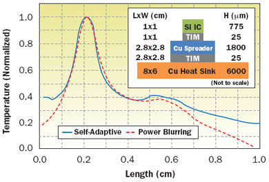
Figure 1. Schematic (inset) of pyramid structure and comparison of normalized temperature distributions along cut A-A in Figure 1 obtained with the current self-adaptive approach and the power blurring method [10]. Each curve is normalized with its own peak temperature value.
A Representative Example
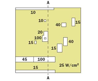
The capabilities of the transient ultra-fast self-adaptive technique are next demonstrated on a representative problem, consisting of five centered blocks stacked as shown schematically in the inset of Figure 1. This problem has been previously solved by the power blurring technique and compared to corresponding results obtained with the commercial software ANSYS [10]. As argued in [10], high spatial resolution is required to correctly simulate the thermal behavior of hot spots in the micron regime; otherwise, chip temperatures can be drastically underestimated. High-resolution simulations with traditional methods require sophisticated grid generation and can be computationally prohibitive, particularly in the presence of a complex power distribution with numerous heat sources. To simulate this complexity and the presence of various active devices, the power distribution shown in Figure 2 is applied on the top silicon layer.
 |
Figure 2. Power distribution map applied to the surface of the silicon IC block [10].
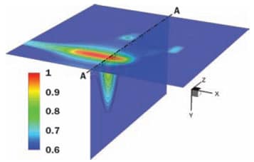
The steady-state solution of the full three-dimensional problem for a prescribed accuracy of 1% was obtained in 13 s on a 3 GHz Pentium 4 PC with 3 GB of RAM. The thermal behavior of a representative subset of the entire structure is shown in Figure 3 where contour field distributions are plotted on the top horizontal plane of the IC (10×10 mm2) and one vertical plane dropping from cut A-A (10×1 mm2). To compare with the results of the power blurring method, temperature values were extracted on a line running along the middle of the top Si IC (cut A-A in Figure 2). The normalized temperature results plotted in Figure 1 show good agreement except toward the edges of the Si block where the absence of an adiabatic condition in the power blurring method leads to the lower temperatures. By sub-resolving the physics over several orders of magnitude changes in spatial scales, the self-adaptive method is capable of capturing the fine details of the heat sources. This is particularly evident in the region of the second peak in Figure 1 and in the temperature contours on the horizontal map in Figure 3. The accurate simulation of this simple pyramid structure is useful to demonstrate that the ultra-fast self-adaptive method can resolve all details associated with heat sources and features using minimal computational resources, not only on a surface but also throughout the three-dimensional structure.
Figure 3. Temperature rise maps (normalized with overall peak value): horizontal on top of Si surface; vertical for a slice 1000 �m deep.
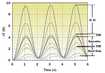
A further advantage of the self-adaptive method is its ability to resolve thermal transients within complex three-dimensional structures. As an example, the power distribution in the pyramid problem above was modulated sinusoidally and solved over three pulse cycles. The complete solution required 12 CPU minutes. The prescribed accuracy was 1%, signifying that the solution would have changed by less than 1% had both the spatial and the temporal resolutions been doubled. The self-adaptive nature of the present approach also implies that no additional, computationally expensive, convergence studies are required to ensure that the obtained solution is grid and time step independent. In fact, once a solution is obtained to within the specified error threshold, the solution is in effect grid and time step independent within that error. A useful way to explore the thermal response of the structure is to observe the transient temperature behavior at different depths. A total of eleven probing points were selected along a vertical line that starts from the middle of the large 100 W/cm2 source, which is also the hottest point on the surface of the IC. The eleven points were located at the top, middle, and bottom of the five material layers making up the structure. Figure 4 compares the temperature responses at these locations. The thermal inertias of the various materials in the structure account for the visible time shift in the location of the peak temperature, both within each pulse as well as across pulses. Also, one can observe that the average temperature increases since the structure does not have sufficient time to return to the ambient level.
 |
Figure 4. Transient response of temperature rise for three sine pulses at 11 locations through the depth of the full structure.
Conclusions
Heat is an unavoidable byproduct in electronics and can be the limiting factor at submicron scales. Temperature is the primary indicator in heat management, and thus temperature knowledge is critical in guiding design, gauging performance, and identifying failure. Experimental methods are important and necessary means for obtaining temperature fields. With careful attention paid to random and systematic uncertainties, modern optical methods can provide valuable data at points or areas of interest with submicron spatial resolution. Computational methods are also important and can play a key role in thermal characterization, particularly in prototyping and design. As demonstrated in this article, with careful attention given to verification and validation, novel simulation methods can provide transient temperature information in three spatial dimensions and in critical regions that are inaccessible to measurement tools. In conclusion, the self-adaptive method demonstrated above is highly computationally efficient; automates the challenging grid generation process; provides built-in grid convergence; ensures that material, power, and geometric features are resolved; can handle several orders of magnitude changes in spatial and temporal scales; and provides a full three-dimensional thermal solution to within a specifiable temperature accuracy.
References
- Raad, P.E., Komarov, P. L., and Burzo, M. G., “Thermo-Reflectance Thermography for Submicron Temperature Measurements,” ElectronicsCooling, Vol. 14, Feb 2008, pp. 28-29.
- Joshi, Y., Baelmans, M., Copeland, D., Lasance, C. J. M., Parry, J., and Rantala, J., “Challenges in Thermal Modeling of Electronics at the System Level: Summary of Panel held at the Therminic 2000,” Microelectronics Journal, Vol. 32, 2001, pp. 797-800.
- Rosten, H. I., Lasance, C. J. M., and Parry, J. D., “The World of Thermal Characterization According to DELPHI-Part I: Background to DELPHI,” IEEE Transactions on Components, Packaging, and Manufacturing Technology, Vol. 20, 1997, pp. 384-391.
- Raad, P.E., Komarov, P. L., and Burzo, M. G., “Non-Contact Surface Temperature Measurements Coupled with Ultrafast Real-Time Computation,” Proc. 23rd SEMI-THERM, San Jose, CA, 2007, pp. 57-63.
- Celik, I. B., Ghia, U., Roache, P. J., Freitas, C. J., Coleman, H. and Raad, P. E., “Procedure for Estimation and Reporting of Uncertainty Due to Discretization in CFD Applications,” ASME Journal of Fluids Engineering, Vol. 130, 2008.
- Raad, P. E., Wilson, J. S., and Price, D. C., “System and Method for Predicting the Behavior of a Component,” U.S. Patent No. 6,064,810 (2000), Korean Patent No. 0501053 (2005), Japanese Patent No. 3,841,833 (2006).
- Wilson, J. S. and Raad, P. E., “A Transient Self-Adaptive Technique for Modeling Thermal Problems with Large Variations in Physical Scales,” International Journal of Heat and Mass Transfer, Vol. 47, 2004, pp. 3707-3720.
- Raad, P.E., Komarov, P. L., and Burzo, M. G., “Thermal Characterization of Embedded Electronic Features by an Integrated System of CCD Thermography and Self-Adaptive Numerical Modeling,” Microelectronics Journal, Vol. 39, 2008, pp. 1008-1015.
- Raad, P.E., “Thermography Measurement System for Conducting Thermal Characterization of Integrated Circuits,” U.S. Patent No. 7,444,260 (2008).
- Park, J.-H., Wang, X., Shakouri, A., and Kang, S.-M., “Fast Computation of Temperature Profiles of VLSI ICs with High Spatial Resolution,” Proc. 24rd SEMI-THERM, San Jose, CA, 2008, pp. 50-54.


