Introduction
Because of substantial increases in the power density of electronic packages over the past few decades, thermal interface resistance can comprise more than 50% of the total thermal resistance in current high-power packages [1]. Unless advanced thermal interface materials (TIMs) that achieve order-of-magnitude improvements in performance quickly emerge in the market, the portion of the thermal budget spent on interface resistance will continue to grow because die-level power dissipation densities are projected to exceed 1 W/mm2 (100 W/cm2) within the next 10 years [2]. Fortunately, improved understanding of heat transfer at nanometer scales, combined with increased ability to design new materials at the atomic level, has enabled a broad range of technological advances that can be applied to develop TIMs with performance characteristics that keep pace with cooling demands as electronics continue to evolve along Moore’s law.
Carbon nanotubes (CNTs) are honeycomb-like (i.e., hexagonally shaped) arrangements of carbon atoms that are rolled into cylindrical tubes with diameters as small as a few atoms wide and aspect ratios as high as 105. Because of these unique structural features and strong carbon-to-carbon bonding, CNTs possess many exceptional vibrational, optical, mechanical, and thermal properties that have been utilized in myriad applications. CNTs can be produced from a wide variety of processes, such as arc-discharge, pyrolysis of hydrocarbons over metal nanoparticles (e.g., in Chemical Vapor Deposition (CVD) or plasma-enhanced CVD processes), and laser vaporization of graphite targets, to name a few prominent methods. Considerable attention has been focused on developing advanced TIMs that utilize the extraordinarily high axial thermal conductivity of CNTs – theoretical predictions suggest values as high as 3000 W/mK [3] and 6600 W/mK [4] for individual multiwalled CNTs and single-wall CNTs, respectively. Early studies focused on dispersing CNTs in a compliant polymer matrix to enhance the effective thermal conductivity of the composite structures [5]. Yet, only modest improvements in thermal performance were achieved because enhancement of thermal conductivity in such structures is hindered by thermal interface resistance between CNTs and the matrix and mechanical stress at CNT-matrix boundaries that reduces the speed at which phonons propagate in the CNTs (i.e., the surrounding elastic medium alters phonon dispersion and reduces the intrinsic thermal conductivity in CNTs) [6]. While limited in comparison to dry CNT TIM structures as discussed below, CNT-polymer composites remain an active research focus and several companies are developing products based on this technology as highlighted in a recent article [7].
Over the past five years, significant attention has shifted to vertically oriented CNT arrays (a.k.a. CNT forest, mats, or films) as promising TIM structures that have been demonstrated to produce contact resistances that compare favorably to state-of-the-art materials [8]. Such configurations possess a synergistic combination of high mechanical compliance and high effective thermal conductivity — in the range of 10-200 W/mK [9-11]. The conformability feature is particularly advantageous in addressing mismatches in coefficients of thermal expansion that can cause TIM delamination and device failure. Also, in contrast to polymer-CNT composites and the best thermal greases, CNT array interfaces are dry and chemically stable in air from cryogenic to high temperatures (~ 450°C), making them suitable for extreme-environment applications [12].
It is important to note that all CNT array TIMs are not created equal; as a result, performance can vary greatly and depends on many factors, e.g., array density and height, CNT diameter, CNT quality, the adhesion of CNTs to the growth substrate, etc. However, since the first investigations of the efficacy of CNT arrays as TIMs, substantial improvements in metrology and synthesis control have led to lower thermal resistances and less scatter in reported values. The purpose of this article is to present and discuss recently published data on the performance of various CNT array TIMs that produce resistances that are near or below the range of resistances achieved by the best materials used today. The article highlights important characteristics, current performance bottlenecks, and significant technical considerations for integrating CNT array TIMs with real devices.
Heat transfer through CNT Array Interfaces
The most actively studied CNT array interface structure is the one-sided CNT array interface that consists of CNTs directly grown on one substrate with CNT free ends in contact with an opposing substrate (see Figure 1). The numerous CNT contacts at both substrates form parallel heat flow paths within the framework of the thermal resistance network illustrated in Figure 1. This network shows thermal resistances resolved at the individual nanotube level for true CNT-substrate interfaces, both at the growth substrate (with a nanotube number density of N, in contacts/area) and at the opposing interface (with a contacting nanotube number density of n). The resistance at each local CNT-substrate contact can be modeled as two resistances in series [13]: 1) a classical substrate constriction resistance (R cs) and 2) a resistance (Rb) that results from the ballistic nature of phonon transport through contacts much smaller than the phonon mean free path in the materials (~ 100 nm). The ballistic resistance (Rb) is usually orders of magnitude larger than Rcs for CNT-substrate contacts, which are typically on the order of 10 nm.
The remaining resistance (R”array) is from heat conduction through the CNT array. This effective resistance is defined for the entire array (including void spaces) to simplify the modeling effort. Moreover, this quantity has been measured in prior work for representative samples and can be used to interpret experimental results that only measure overall thermal interface resistance. When array height is less than 50 μm, R”array is usually negligible in comparison to the resistances at the CNT-substrate contacts [13].
Given knowledge of the contact number densities at the growth substrate (N) and the opposing substrate (n), an overall or total interface resistance can be calculated. The former density (N) can be estimated from scanning electron micrographs of synthesized arrays, and the latter density (n) can be estimated using a recent model that predicts real contact area in CNT array interfaces as a function of applied pressure and important array characteristics, such as porosity and CNT diameter [13]. The model reveals that fabricating arrays with low effective compressive modulus is critical for establishing large interfacial contact and minimizing total thermal resistance. A detailed development of the CNT array TIM resistor network model is presented elsewhere [13]. Applying the model to one-sided CNT array interfaces with a surface density of 108 CNTs/mm2 and CNT diameters of 20 nm suggest that total resistances of ~ 0.1 mm2K/W represent limiting values that could be achieved if the CNTs are completely and perfectly contacted and have well-matched acoustic impedances at all CNT-substrate interfaces.
CNT Array TIMS
The three CNT array TIMs shown in Figure 2 have exhibited some of the most promising thermal performance characteristics to date. The first is the one-sided interface structure discussed above. The second configuration, i.e., the two-sided configuration, consists of CNT arrays adhered to surfaces on both sides of the interface and brought together in VelcroTM-like contact (in this configuration CNTs mechanically entangle and are attracted to each other by van der Waals forces). The third structure comprises vertically oriented CNT arrays directly and simultaneously synthesized on both sides of thin foil substrates that are inserted into an interface. The CNT-coated foil structures are particularly attractive in that they serve as a method for applying CNT arrays to interfaces between heat sinks and devices that would experience damage from exposure to the high temperatures normally required for high-quality CNT growth (> 700°C).
Using CVD processes that are ubiquitous in the electronics industry, the CNT array TIMs in Figure 2 have been grown on various substrates such as silicon, silicon carbide, copper, and aluminum that are important for thermal management applications [8]. Based on conversations with a few companies that have demonstrated production-level growth of CNT arrays in large-scale CVD reactors, it is estimated that the CNT TIMs in Figure 2 can be made for significantly less than $1 per TIM (assuming an area of 2 cm2 for each TIM), which is cost competitive with currently available TIMs; however, achieving sufficient process control in production-scale environments remains a technical barrier to market entry.

Thermal Resistances of CNT Array TIMS
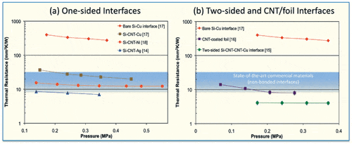
Figure 3 summarizes the performance of one-sided, two-sided, and CNT-coated foil interfaces as a function of pressure [14-19]. One-sided interfaces have achieved resistances as low as 7 mm2K/W [14], and two-sided interfaces have been demonstrated to produce resistances as low as 4 mm2K/W [15] — this value is comparable to the resistance of a soldered interface. For both of these configurations, the pressure dependence is weak in the measured range because the CNTs are compressed near their maximum extent within the measurement range [13]. Resistances as low as 8 mm2K/W were produced with the CNT-coated foil TIMs [16]. The CNT-coated foils enhance real contact area significantly, which results in low contact resistance, because deformation of the thin foil substrate “assists” CNT displacement to match the topology of the mating surfaces.
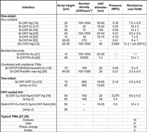
There are considerable data on the performance of CNT array TIMs at a single pressure [20-26]. These data are summarized in Table 1 along with the lowest resistances achieved in measurements as a function of pressure. To demonstrate performance at operating temperatures for a variety of devices, the resistances of the one-sided SiCCNT-Ag interface in Table 1 were measured from room temperature to 250°C and the values were approximately steady in this range [12]. A few groups have explored techniques to improve CNT-substrate bonding and contact area, particularly at the interface created by free CNT ends. Bonding free ends [21, 22], or combining CNT arrays with traditional TIMs that wet the interface well (e.g., phase change materials) [19, 26], produced thermal resistances that were an order of magnitude lower than the resistances of one-sided interfaces in dry contact. These results are also presented in Table 1.
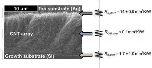
A few groups have measured thermal resistances of CNT array TIMs using transient techniques that allow the true CNT-substrate resistances and the resistance of the CNT array to be independently resolved [15, 21, 22]. Such measurements confirm that the resistances at CNT-substrate contacts are much larger than the intrinsic resistance of the CNT array, and that the resistance at the interface between CNT free ends and an opposing substrate is considerably larger than the resistance at the CNT-growth substrate interface — the true contact area established by weakly bonded van der Waals forces between CNT free ends. And the opposing substrate is considerably less than the contact area at well anchored CNT roots. Figure 4 illustrates a one-sided interface with local resistances at true CNT-substrate contacts highlighted. The resistance between CNT free ends and the opposing substrate is clearly the largest resistance in the network. The thermal resistances at the CNT free ends also comprise the largest percent of total resistance in the two-sided and CNT-coated foil configurations [15, 16].
CPU Burn-In with CNT Array TIMS
Recently, CNT-coated foil TIMs were characterized in an industry typical burn-in tester that used a current-generation Intel CPU [29]. The TIMs consisted of CNTs grown on one side of 25 μm-thick copper foil with CNT free ends in contact with a heat sink and the bare foil surface in contact with the die. The CNT-coated foil TIMs were tested for 1000 thermo-mechanical cycles. They produced resistances at least 30% lower than the resistances produced by a variety of bare foil TIMs (Cu, Al, etc.). These performance improvements were consistent over all tested cycles, and CNTs remained well adhered to the foils after removal from the interfaces. Compared to the resistances produced by state-of-the-art materials used for CPU burn-in, a twofold improvement in system resistance was achieved when paraffin wax was added to the CNT-coated TIMs [29].


CONCLUSIONS
To date, three CNT array TIM configurations have been developed to the point where they produce resistances that compare favorably to the best TIMs currently in use. So far, the lowest resistances produced by CNT array TIMs are on the order of 1 mm2K/W. Further improvements can be achieved by optimizing the compliance of CNT arrays to maximize the real contact area in the interface. Experimental data and theoretical predictions reveal that the resistances at CNT-substrate contacts severely limit the potential of CNT array TIMs. Improvements in bonding and thermal transport at these contacts can lead to substantial reductions in resistance, approaching estimated theoretical limits of ~ 0.1 mm2K/W.
- Cola, B.A., Xu, J., Cheng, C., Xu, X., Hu, H., Fisher, T.S., “Photoacoustic Characterization of Carbon Nanotube Array Thermal Interfaces,” Journal of Applied Physics, Vol. 101, 2007, p. 054313.
- Cola, B.A., Xu, X., Fisher, T.S., “Increased Real Contact in Thermal Interfaces: A Carbon Nanotube/Foil Material,” Applied Physics Letters, Vol. 90, 2007, p. 093513.
- Xu, J., Fisher, T.S., “Enhanced Thermal Contact Conductance Using Carbon Nanotube Array Interfaces,” IEEE Transactions on Components and Packaging Technology, Vol. 29, 2006, pp. 261-267.
- Xu, Y., Zhang, Y., Suhir, E., Wang, X., “Thermal Properties of Carbon Nanotube Array Used for Integrated Circuit Cooling,” Journal of Applied Physics, Vol. 100, 2006, p. 074302.
- Xu, J., Fisher, T.S., “Enhancement of Thermal Interface Materials with Carbon Nanotube Arrays,” International Journal of Heat and Mass Transfer, Vol. 49, 2006, pp. 1658-1666.
- Amama, P.B., Cola, B.A., Sands, T.D., Xu, X., Fisher, T.S., “Dendrimerassisted Controlled Growth of Carbon Nanotubes for Enhanced Thermal Interface Conductance,” Nanotechnology, Vol. 18, 2007, p. 385303.
- Tong, T., Zhao, Y., Delzeit, L., Kashani, A., Meyyappan, M., Majumdar, A., “Dense Vertically Aligned Multiwalled Carbon Nanotube Arrays as Thermal Interface Materials,” IEEE Transactions on Components and Packaging Technology, Vol. 30, 2007, pp. 92-99.
- Panzer, M., Zhang, G., Mann, D., Hu, X., Pop, E., Dai, H., Goodson, K.E., “Thermal Properties of Metal-Coated Vertically Aligned Single-Wall Nanotube Arrays,” ASME Journal of Heat Transfer, Vol. 130, 2008, p. 052401.
- Zhang, K., Chai, Y., Yuen, M.M.F., Xiao, D.G.W., Chan, P.C.H., “Carbon Nanotube Thermal Interface Material for High-Brightness LightEmitting-Diode Cooling,” Nanotechnology, Vol. 19, 2008, p. 215706.
- Wang, H., Feng, J., Hu, X., and Ng, K.M, “Synthesis of Aligned Carbon Nanotubes on Double-Sided Metallic Substrates by Chemical Vapor Deposition,” Journal of Physical Chemistry C, Vol. 111, 2007, pp. 1261712624.
- Liu, X., Zhang, Y., Cassell, A.M., and Cruden, B.A., “Implications of Catalyst Control for Carbon Nanotube Based Thermal Interface Materials,” Journal of Applied Physics, Vol. 104, 2008, p. 084310.
- Cola, B.A., Hodson, S.L., Xu, X., and Fisher, T.S., “Carbon Nanotube Array Thermal Interfaces Enhanced with Paraffin Wax,” Proceedings of 2008 ASME Summer Heat Transfer Conference, Jacksonville, FL, 2008.
- Prasher, R., “Thermal Interface Materials: Historical Perspective, Status, and Future Directions,” Proceedings of the IEEE, Vol. 94, No. 8, 2006, pp. 1571-1586.
- Chung, D.D.L., “Materials for Thermal Conduction,” Applied Thermal Engineering, Vol. 21, 2001, pp. 1593-1605.
- Cola, B.A., “Photoacoustic Characterization and Optimization of Carbon Nanotube Array Thermal Interfaces,” Ph.D. Dissertation, Purdue University, West Lafayette, IN, 2008.

![Figure_1 Figure 1. (a) Schematic (not to scale) of an interface with the addition of a vertically oriented CNT array of thickness tarray [8]. (b) Buckled CNT contacting an opposing surface with its wall. As shown, some CNTs do not make direct contact with the opposing surface. (c) Resistance schematic of a one-sided CNT array interface between two substrates, showing constriction resistances (Rcsi), phonon ballistic resistances (Rbi), and the effective resistance of the CNT array (R”array).](https://electronics-cooling.com/wp-content/uploads/2010/04/Figure_1.gif)
![Figure_2 Figure 2. CNT array interface structures: (a) example of one-sided interface; (b) example of two-sided interface, (c) example of CNT-coated foil interface, (d) CNT arrays on both sides of 25 μm-thick Al foil [8].](https://electronics-cooling.com/wp-content/uploads/2010/04/Figure_21.gif)


