Peter E. Raad
Southern Methodist University and TMX Scientific, Inc., Dallas, Texas
A recent news item [1] described the intended efforts of researchers from IBM, EPFL, and ETH to “keep Moore’s Law for another 15 years.” Doing so, the article adds, “will require a change from mere transistor scaling to novel packaging architectures such as so-called 3D integration, the vertical integration of chips.” The four-year collaborative project called CMOSAIC will investigate cooling techniques that can support a 3D architecture, including “the use of hair-thin, liquid cooling microchannels measuring only 50 microns in diameter between the active chips.” The researchers from industry and academia will undoubtedly use myriads of experimental and computational methods to devise their approaches, design their solutions, construct their prototypes, and ultimately test the merits of their hypotheses. This is consistent with what we have always done! However, the inevitability of three-dimensionality in integrated circuits [2] raises an interesting question: how will we know what’s happening inside? Whether it is physicians diagnosing and mapping optimal routes for successful surgery or authorities interested in the activities of a suspect operating within the inner confines of a large structure, the problem is the same: how to assess what we cannot access.
Engineers and scientists have long relied on measurements to diagnose system behavior, enlighten thinking, and guide next steps. The dramatic advances in computing machines have made it possible to add numerical simulation as a powerful contributor in our arsenal of investigatory tools for complex systems. Traditionally, though, an individual researcher’s strength would favor one approach over another. More recently as computers have become more potent and software packages have become more accessible, experimentation has become in the minds of some only necessary in so far as it provides validation to numerical models. But the community knows too well the dangers of single-minded approaches to any significant problem at hand. The question is then not whether we need to leverage as many individual approaches as possible — analytical, experimental, and computational — but rather which ones are most appropriate to solve our particular problem at hand, which is to figure out the thermal behavior of buried electronic devices and features of interest. This is not an idle question on the semiconductor roadmap. Without a view into the inner workings of complex devices, we will be blind to the actual performance of our designs, and hence condemned to spending our valuable time and energy on trial-and-error rather than rapid prototyping and iterative refinement.
Let us first consider experimentation as it pertains to this discussion. A measurement has the most important advantage of capturing the actual thermal behavior with all the physics as well as the geometric and material complexities that are influencing the operation of a real device. However, the Zeroth Law of Thermodynamics confines us to having to measure temperature indirectly by calibrating the response of a third body to differing temperature levels. There are a number of useful approaches [3, 4], which can be categorized based on the relationship between the measuring implement and what is being measured. We may speak of invasive and non-invasive, contact and non-contact approaches, and within these, we can refer to methods that rely on material behavior (e.g., mercury thermometer, liquid crystal paint), electrical response (e.g., thermocouples, thermistors), optical signature or interference (e.g., infrared, thermoreflectance), to name but a few. Different methods have different strengths, limitations, and figures of merit, e.g., accuracy, resolution (spatial, temporal, and temperature), and precision. Irrespectively, for an implement to record the temperature of a material, the two have to be communicant either physically or optically. Physical contact presents the difficulty of isolating the effect of contact itself, whereas an optical approach limits access to surface or near-surface regions. Given the above, one can now certainly appreciate the challenges of measuring vertically integrated electronic devices, and without even yet considering the additional difficulties presented by the ranges of scales from nanometers to centimeters that are inherent in modern complex devices. Access is a limiting factor.
Computational approaches, on the other hand, do not have issues of physical or optical access. Given a choice of spatial discretization (e.g., finite element/volume/difference) and temporal discretization (e.g., explicit, implicit, trapezoidal), an analyst can construct the computational domain of interest, select the heat transfer physics in play, prescribe initial and boundary conditions, and then wait for the numerical simulation to complete. Of course, (i) different numerical approaches have differing levels of accuracy, stability, and convergence; (ii) numerical simulations cannot represent physics that are not included in the formulation; and (iii) geometric and material complexities can make grid generation quite challenging. The power of computations is that, given an accurate and appropriately convergent solution, we can easily extract the thermal behavior of important features wherever they may be within the computational domain. However, even the most precise and accurate numerical simulations cannot give us results that exceed the fidelity of the input data, be they those associated with the geometry, the material properties, or the heat sources. This is an important point. Numerical simulations can give us gloriously colorful representations of thermal behavior, but only as it pertains to the idealized representation of the device as described by the input data. The numerical results do not automatically comprehend the effects of data uncertainty, natural device aging, or rapid deterioration due to device malfunction. Input data are a limiting factor.
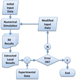
So, on the one hand, experiments can comprehend physics and device complexity, but are restricted to specific locations, and on the other, numerical simulations can provide detailed, transient, 3D behavior, but only insofar as the input data represent the actual device of interest. What if we didn’t have to pick sides? What if we could marry the two approaches to overcome their respective limitations? Consider the notion of what we might call “tuning approaches” that leverage experimental data to guide simulation. This concept is not unique to thermal analysis of semiconductor devices. In a slightly different approach, perhaps better termed “data assimilation,” meteorologists begin by predicting the path of a hurricane starting with a reasonable input data set, but continually modify the progress of the simulation as actual data become available. For our problem at hand, one could imagine simulating a vertically integrated device with the best possible available input data, but then comparing the results in those locations and areas where physical measurements are available in order to generate a more representative input data set. Such an iterative process (Fig. 1) would continue until computations and measurements agree to within an acceptable error [5].

There are two important issues to consider: uniqueness and feasibility. First, when solving partial differential equations, particularly if they are nonlinear, it is possible, even probable to have multiple scenarios yield the same temperature value at some given point. Just because the computational and experimental results agree at one point does not make the solution unique. From an information entropy point of view, however, as the number of points involved in the comparison increases, the probability of uniqueness increases considerably. Indeed, as the number of reference points increases into the hundreds and thousands, the probability of two different well-posed problems producing matching results at all those points becomes infinitely small. Secondly, in order for such an iterative approach to be practical, the numerical simulation has to be very fast. The computational time depends on the chosen resolutions in space and in time as well as on the efficiency of the numerical algorithms used to solve the resulting systems of equations. Setting aside algorithmic efficiency and computer speed, the overall time budget is primarily driven by grid size and time step. A difficulty particular to the thermal modeling of integrated circuits is the range of spatial and temporal scales that must be resolved in order for the simulation to be useful. If the smallest grid size were chosen to be larger than the smallest heat source, the effect of the latter would be lost. If, on the other hand, the smallest geometric and thermal features are appropriately resolved, the problem size can become prohibitively large, making multiple solutions within an optimization approach impractical.

Compact models [6] and ultra-fast numerical approaches [7] have been introduced to reduce computational time by orders of magnitude. Analysts who have at their disposal ultra-fast simulation capabilities become more likely to practice iterative refinement and even experimentally-guided optimization. Additionally, this opens up the interesting possibility of integrating sensors that not only measure locally but also predict thermal behavior in other regions of interest. So then even beyond design and prototyping, highly optimized thermal simulation codes could be embedded within small chips to continually predict internal thermal behavior within operating devices and provide feedback to alter their behavior.

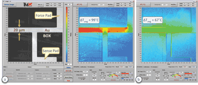
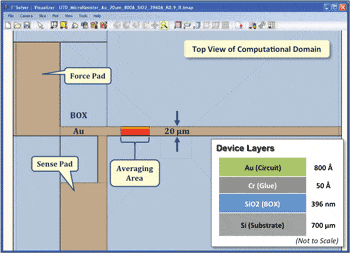
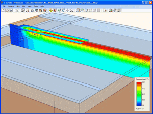
Let’s demonstrate the overall idea with an example. Many commercial and academic laboratories are heavily engaged in the search for new buried oxide materials (BOX) at the semiconductor fabrication level and thermal interface materials (TIM) at the die assembly level. Identifying winning candidates and characterizing their actual, in situ thermal impact is a significant and worthwhile pursuit. Several useful approaches exist for measuring the thermal conductivity (or diffusivity) of materials, e.g., 3-ω [8], flash [9], transient thermoreflectance [10], etc. Thin films present a special challenge for most techniques as does the identification of the contributions of the thermal interfaces, which are invariably process dependent and thus not amenable to generalization [11]. So an interesting example here might be to combine the powers of measurements and computations to extract the actual, effective thermal conductivity of BOX materials. Gold microresistors have been deposited on various metal oxides [12], two of which will be used in this example: Silicon (SiO2) and Aluminum (Al2O3) oxides. Keeping all other conditions identical, we measure the temperature maps with a thermoreflectance-based thermal microscope [5, 13] of the two microresistors (Fig. 2) and calculate an average temperature over a section of each of them. The calculated average temperatures from the SiO2 and Al2O3 devices are 134˚C and 98˚C, respectively. This difference indicates that Al2O3 is a better thermal conductor than SiO2, but does not give us the value of the thermal conductivity of either material. And so we switch to the computational approach, construct a model of, say, the silicon oxide device, and compute with a guessed initial value of the effective conductivity (or diffusivity) of SiO2 (Fig. 3). It would make sense to start with the published value of 1.4 W/m-K and even assume that our material interfaces are perfect. Simulating the conduction heat transfer problem with an ultra-fast, self-adaptive computational engine [7, 13] and calculating an average value over the corresponding area that we measured gives an average surface temperature of 102˚C. This discrepancy of 32˚C (or 24%) guides us to modify our input value downwardly from 1.4 W/m-K. Repeating the simulation with effective thermal conductivities for the SiO2 layer of 1.2, 0.9, and 0.8 W/m-K yields average temperature values of 110˚C (18% lower), 128˚C (5% lower), and 137˚C (2% higher), respectively. A final effective conductivity of 0.83 W/m-K yields the experimentally obtained average temperature of 134˚C. The deduced value for the effective thermal conductivity of thermally grown silicon oxide coincides well with previous measurements obtained with a purely experimental technique [14]. Each of these converged transient computations required just 23 seconds of CPU time on a
3 GHz Pentium 4 desktop computer. Of course, the reader is immediately aware that this approach can be automated and that other important geometric and physical parameters can be included in the optimization process. The purpose of this basic example was simply to step through the optimization process and to demonstrate the power and usefulness of coupling experimental and computational approaches.

We must remain open to and work toward breakthroughs in metrology. A groundbreaking non-invasive technology, such as what happened with CT-Scan or MRI for seeing within the human body, could come along to enable us to measure temperatures deep within 3D devices. But in the meantime, we need to try to fully leverage what we already have. Extending the life of Moore’s Law is a good enough reason.
References
“What’s Happening: 3D Chip Stacking Will Take Moore’s Law Past 2020, Pose New Challenges,” ElectronicsCooling, Vol. 16, 2010, p. 28.
Cale, T.S., Lu, J.Q., and Gutmann, R.J., “Three-Dimensional Integration in Microelectronics: Motivation, Processing, and Thermomechanical Modeling,” Chemical Engineering Communications, Vol. 195, 2008, pp. 847–888.
Childs, P.R.N., Greenwood, J.R., and Long, C.A., “Review of Temperature Measurement,” Review of Scientific Instruments, Vol. 71, No. 8, 2000, pp. 2959-2979.
Farzaneh, M., Maize, K., Lüerßen, D., Summers, J.A., Mayer, P.M., Raad, P.E., Pipe, K.P., Shakouri, A., Hudgings, J.A., and Ram, R., “CCD-Based Thermoreflectance Microscopy: Principles and Applications,” Journal of Physics D: Applied Physics, Vol. 42, 2009, pp. 143001-143021.
Raad, P.E., Komarov, P.L., and Burzo, M.G., “An Integrated Experimental and Computational System for the Thermal Characterization of Complex Three-Dimensional Submicron Electronic Devices,” IEEE Transactions on Components and Packaging Technologies, Vol. 30, 2007, pp. 597-603.
Lasance, C.J.M., “Ten Years of Boundary-Condition-Independent Compact Thermal Modeling of Electronic Parts: A Review,” Heat Transfer Engineering, Vol. 29, 2008, pp. 149–168.
Wilson, J.S. and Raad, P.E., “A Transient Self-Adaptive Technique for Modeling Thermal Problems with Large Variations in Physical Scales,” International Journal of Heat and Mass Transfer, Vol. 47, 2004, pp. 3707-3720.
Cahill, D. G., “Thermal Conductivity Measurement from 30 to 750 K: the 3ω Method,” Review of Scientific Instruments, Vol. 61, 1990, pp. 802-809.
Parker, W.J., Jenkins, R.J., Butler, C.P., and Abbott, G.L., “Flash Method of Determining Thermal Diffusivity, Heat Capacity, and Thermal Conductivity,” Journal of Applied Physics, Vol. 32, 1961, pp. 1679-1684.
Komarov, P.L., and Raad, P.E., “Performance Analysis of the Transient Thermo-Reflectance Method for Measuring the Thermal Conductivity of Single Layer Materials,” International Journal of Heat and Mass Transfer, Vol. 47, 2004, pp. 3233-3244.
Lasance, C.J.M., Murray, C., Saums, D., and Rencz, M., “Challenges in Thermal Interface Material Testing,” Proceedings of the 22nd IEEE SEMI-THERM Symposium, Dallas, TX, 2006.
Lee, T., Aliev, A., Burzo, M., Komarov, P., Raad, P., and Kim, M., “New SOI Substrate with High Thermal Conductivity for High Performance Mixed-Signal Applications,” 218th Electrochemical Society (ECS) Meeting, Las Vegas, NV, Oct. 2010.
T°Imager™ and T°Solver™ are registered trademarks and products of TMX Scientific, Inc.
Burzo, M.G., Komarov, P.L., and Raad, P.E., “Thermal Transport Properties of Gold-Covered Thin-Film Silicon Dioxide,” IEEE Transactions on Components and Packaging Technologies, Vol. 26, 2003, pp. 80-88. l


