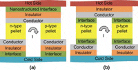
- (a) A nanostructured interface material is used around the module; (b) a nanostructured interface material is used between the thermoelectric material and metal leads.
Semiconductor Research Corporation (SRC) and researchers from Stanford University have developed a novel combination of elements that yields a nanostructure material for packaging. The advance could mean improvements for semiconductors in the form of packaging for devices. Presently, manufacturers must rely on tiny pins or thick solder to bond sections of the semiconductor in order for the device to perform. However, current solder materials tend to degrade and fail due to heat and mechanical stress. In order to continue the scaling of integrated circuits, SRC and Stanford have researched materials that provide a high thermal connectivity — comparable to copper — with the flexible compliance of foam, the researchers say. The answer has been created through a nanostructured thermal tape that conducts heat like a metal while allowing the neighboring materials to expand and contract with temperature changes (metals are too stiff to allow this). This ability to reduce chip temperatures while remaining compliant is a key breakthrough for electronic packaging.


