These days, many thermal engineers face the challenge of defining effective heat sink cooling solutions for high power processors and ASICs (Application-Specific Integrated Circuits). The usual practice would be to calculate a value of ΘJA (junction-to-air thermal resistance) for the combined package/heat sink assembly and compare it to the requirements of the application.
Traditionally, in performing this sort of calculation, one would first obtain a value of ΘJC (junction-to-case thermal resistance) from the packaging supplier and a value of ΘSA (sink-to-air thermal resistance) from the heat sink supplier. Since the heat sink test is usually performed with a uniform heat flux applied over the entire base, one would need to correct the value of ΘSA, assuming that the heat is transferred into the heat sink uniformly over the entire contact area between the package and the heat sink. A very accurate and efficient method of doing this has been described in this publication [1]. One would then make assumptions about the thickness and thermal conductivity of prospective thermal interface materials (TIMs) to provide effective thermal contact between the package and the heat sink. The thermal resistance of this particular TIM, between the package case and the heat sink base (namely, TIM2) is referred to as ΘCS.
The three thermal resistance values would then be added up to obtain the desired value of ΘJA per the following expression:
ΘJA = ΘJC + ΘCS + ΘSA (1)
This procedure worked well enough when power levels were lower than today. The accompanying higher values of thermal resistance masked the presence of certain thermal interactions that are important sources of error for high power/low thermal resistance components. The fact that these resistances are not boundary-condition independent means that their precise value depends upon the details of the heat transfer between the various components [2]. This is due to the fact that these thermal resistance metrics are the product of a methodology which ultimately represents a measurement approach: namely the temperatures TJ, TC, TS, all are determined at the geometric center of each component [3]. Such single-point temperature measurements do not provide direct information regarding the heat flux distribution that could be useful in defining a more robust thermal resistance metric.

Summary of Part 1
Part 1 of this article was devoted to exploring the nuances of the interactions between these components, particularly as to their effect on the heat flux distribution in the path between the package case and the heat sink base [4].
Figure 1 depicts a typical configuration of a flip-chip cavity package containing a copper lid in contact with the base of a heat sink. Those components depicted using bold colors are explicitly represented in the Finite Element Analysis (FEA) model. These constitute the primary heat flow path, from the chip to the heat sink. Those drawn with the faint colors are present in the physical assembly, but are not explicitly represented in the model. These include the heat sink fins and the package substrate and the printed circuit board (PCB) to which the package is electrically interconnected. The cooling effect of the fins is accounted for by the use of an effective heat transfer coefficient (hEFF) applied to the top of the heat sink base. The heat flow through the package substrate to the PCB is simply ignored, since in a high-power package, it is of secondary importance.
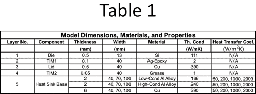
Table I defines the package construction and the variations in the heat sink design explored. The heat sink designs and the large spread in hEFF represent a wide range of thermal performance.
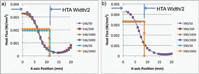
The curved data sets in Figure 2 demonstrate the heat flux distribution through the TIM2 material determined for the lowest and highest conductivity heat sinks, at a value of heat sink width, wHS = 70 mm, and over the full range of hEFF. They show that, even for a package with a 1 mm thick lid made of pure copper, the heat flux is concentrated in the center of the package, in stark contrast to the traditional assumption of uniform heat flow over the package area.
The rectilinear data sets represent a uniform flux distributed over a specified area defined herein as the Heat Transfer Area (HTA). The HTA was defined in Part 1 as: the area bounding a uniform flux region which produces the same value of ΘSA as the FEA simulation with non-uniform flux distribution, each with the same total power. This procedure was decided upon because of its simplicity, rather than pursuing the more involved process of analyzing the actual flux distributions. For a square shaped die and package, such as in the current example, it is convenient to refer to the HTA Width, which provides a more intuitive sense of the size of the area than referring to the area itself.

Derivation and Use of the HTA Concept
Figure 3 shows curves of ΘSA versus the full range of values of HTA Width possible with the present package: from the die width (13 mm) to the full package width (40 mm). These curves were calculated using FEA with only the heat sink base in the solid model and applying the flux at HTA values equal to 13, 20, 30, and 40 mm sq. (Note that this calculation could have been performed with equal accuracy using the method in Ref 1.) The curves were created using a 3rd-order linear regression technique.

The symbol overlapping each curved line represents a value of HTA which yields a value of ΘSA equal to that calculated in the full FEA model of the package in contact with the heat sink. A spreadsheet solver was used in the calculation. For the low conductivity heat sink they are clustered in the range of HTA Widths between 20 and 24 mm. For the high conductivity heat sink they are in the narrower range between 17 and 18 mm.
It is reasonable to expect that the HTA concept should be useful in the calculation of ΘCS, as suggested by a comparison of the uniform flux distribution over the HTA and the actual flux distribution in Figure 2. Since the flux is assumed to be uniform within the HTA, the following expression, representing 1-dimensional heat flow, can be used to calculate ΘCS

where tTIM2 and kTIM2 are the thickness and thermal conductivity of TIM2, respectively. ΘCS is plotted as a function of HTA in Figures 3a and 3b. It is useful to compare the magnitude of ΘCS and ΘSA for the two heat sinks studied. For the low conductivity heat sink, ΘCS is much lower than the lowest value of ΘSA. In the case of the high conductivity heat sink, ΘCS is comparable in magnitude to the lowest values of ΘSA. This fact will be relevant during the error analysis.
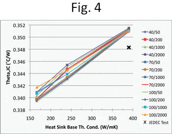
Fig. 4 Plot of ΘJC versus vs kHS at specific values of wHS and hEFF: extracted from full package/heat sink FEA simulation. Black X symbol represents simulated JEDEC test result.
Figure 4 shows the calculated values of ΘJC, plotted versus the heat sink thermal conductivity, kHS, for all the cases studied. It also displays a value of ΘJC, calculated under simulated JEDEC-standard conditions (water-cooled cold plate, 2 mm-thick copper top plate) [5]. Note this is a bit lower in magnitude (0.002 ˚C/W) than the values of ΘJC calculated for the package in contact with the copper heat sink, due to its greater thickness (6 mm vs. 2 mm). ΘJC values calculated for the lowest conductivity heat sink are about 0.01 ˚C/W less than the simulated test value. Comparing these differences with the values of ΘSA and ΘCS in Figure 3 suggest that these deviations in ΘJC in the full model from the simulated test value will not be a significant source of error.
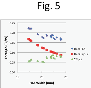
Fig. 5 Plot of ΘCS versus HTA. Blue symbols: values extracted from full package/heat sink FEA simulation. Red symbols: values calculated from Eqn. 2.
Figure 5 contains a plot of ΘCS versus HTA Width. The values of ΘCS were calculated using one of two methods: 1) extraction from the full package/heat sink FEA simulation and 2) calculation using Eqn. 2 and the values of HTA calculated using the method illustrated in Figure 3. The HTA-calculated values are approximately 0.08 ˚C/W less than the FEA-calculated values for the low conductivity heat sinks and 0.05 ˚C/W less for the high conductivity heat sinks. Comparing these discrepancies with the values of ΘSA in Figure 3, suggest that this will be a more significant source of error.
Simplified Theta, JA Calculations Using the HTA Concept
It is hoped that the preceding analysis has made it clear that the assumed size of the area bounding the heat flow between the package and the heat sink has a significant influence on the resultant values of ΘCS and ΘSA and, consequently, ΘJA. This section will explore the accuracy of analytic calculations making various assumptions regarding the size of this bounding area.
Table 2 describes four methods, which differ in this assumption.
• Method #1 assumes the bounding area = the package area.
•Method #2 assumes the bounding area = a single value of HTA averaged over all the cases studies.
•Method #3 assumes the bounding area = average of HTA calculated for each of 3 heat sink configurations.
•Method #4 assumes the bounding area = the specific value of HTA calculated individually for each case.
QJA is calculated using Eqn. 3:
ΘJA= ΘJC,TEST + ΘCS(Area) [Eqn. 2] + ΘSA(Area) [Ref. 1] (3)
The results calculated using each method were compared to the ΘJA values calculated using the original FEA model. A complete listing of all the ΘJA results is provided in Table 2 of Part 1 of this article [4]. The results are shown in Figure 6. The error is summarized in Table 2.
All the methods show an increase in the absolute error as the value of ΘJA gets smaller. Method #1, using the package size for the heat transfer area, has an error of less than 10% for values of ΘJA of 3 ˚C/W and greater. For ΘJA values of less than this, the error grows to 36%. Using the average HTA value of 20.6 mm, in Method #2 leads to a large reduction of error, with the maximum error equal to 16%. Further improvement is obtained with Method #3, using the value of HTA averaged for each heat sink design. Here the maximum error is 10%. Method #4, with a separate value of HTA applied to each case represented a small improvement with the maximum error equal to 9%. As indicated earlier, most of the error in Methods #4 and 5 is due to the ΘCS term.
Conclusions
The past practice of assuming a uniform heat flow between a package and heat sink over the full area of the package is shown to be inadequate with high-power packages. The HTA method uses the same assumption of a uniform flux as before, but uses a value for the bounding area determined from a detailed finite element analysis of the package and heat sink. For this method to become more widely useful, correlations are needed to generate appropriate HTA values for arbitrary package and heat sink designs. Once the appropriate HTA is on hand, then the remainder of the calculation is straightforward.
Note: The method described is only valid for the situation discussed: a single source with its individual heat sink, and cannot be applied to other situations involving multiple sources on one PCB, heat sink or cold plate.

The reader should be reminded that this sort of analysis can be very useful in the early design phase of a project. It has value in generating a preliminary performance specification for a heat sink and TIM2 to accompany the high-power chip and package of interest. Of course, in the final design phase, additional details such as the actual chip power map, the influence of other heat sources and the heat transfer through the package substrate must be accounted for in a detailed numerical model of the package, heat sink, and the system.
References
[1]. Lee, S., “Calculating Spreading Resistance in Heat Sinks,” ElectronicsCooling, Vol. 4., No. 1, January 1998.
[2]. Lasance, C., “Heat Spreading: Not a Trivial Problem,” ElectronicsCooling, Vol. 14, No. 2, May, 2008.
[3]. JEDEC Standard, JESD-12, “Guidelines for Reporting and Using Electronic Package Thermal Information.” Available for free download at
www.jedec.com.
[4]. Guenin, B., “Thermal interactions Between High-Power Packages and Heat Sinks, Part 1, ElectronicsCooling, Vol. 16, No. 4, Winter, 2010.
[5]. JEDEC Standard, JESD-14, “Transient Dual Interface Test Method for the Measurement of the Thermal Resistance Junction to Case of Semiconductor Devices with Heat Flow Through a Single Path.” Available for free download at www.jedec.com. l


