K. Yazawa and A. Shakouri
Baskin School of Engineering, University of California at Santa Cruz, California
Both the miniaturization of electronic and optoelectronic devices and circuits and the increased operation speeds of electronic devices have exacerbated localized heating problems. Steady-state and transient characterization of temperature distribution in devices and interconnects are important for performance and reliability analysis. In this paper we review recent developments in ultrafast submicron thermoreflectance imaging techniques.
Many properties of materials depend on temperature and they can be exploited for local temperature measurement. Good references explaining different thermal measurement techniques, specifically thermoreflectance imaging, include the early stage review by Cutolo [1], the study on dynamic characterization by Altet [2], work on device circuit focus by Christofferson [3], a simulation combined method by Raad [4], and a review by Farzaneh [5]. Thermoreflectance imaging technique is outlined in the next section followed by examples. For the characterization of active devices, thermal maps can provide useful information about the power dissipation profile, hot spots, and manufacturing or material defects before the device completely fails. Transient thermal imaging can show temperature variation in switching devices under pulsed operation. This can be used to identify buried defects or help to extract the thermal resistance/capacitance network in the device, surrounding regions in the substrate and the package. For optoelectronic devices, an additional scheme is required to separate electro-luminescence and the reflected illumination used for thermoreflectance. To demonstrate this, we will show thermal images of solar cells and LEDs. The CMOS transistor circuits require high spatial resolution. At the same time, the structure of multiple metal layer interconnects makes for difficult characterization of the active device junction temperature. With the through silicon substrate thermal imaging, we directly measure the active transistor region. The spatial resolution is important to characterize very small features such as 500 nanometer diameter copper vias in interconnects. Using electrical resistance measurements alone isn’t enough to identify potentially critical locations that can lead to device failure. The latter typically shows the total series resistance. Electron beam techniques can detect local open circuits once the interconnect fails completely. However, the thermal map can show all of the weak connections and hot spots. Thermal maps have been studied in the submicron scale [6]. More importantly, submicron features respond very quickly due to extremely small thermal mass, thus very fast thermal imaging with short pulses and very low duty cycles can be used to identify the current distribution profile before self-heating and temperature-dependent material properties modify the current path.
Thermoreflectance Imaging
The challenge in obtaining high quality thermal images arises when one considers the magnitude of the weak temperature-dependent reflection coefficient (thermoreflectance effect) in metals and semiconductors. The thermoreflectance coefficient is on the order of 10-4-10-5 per degree Kelvin for most materials [7]. This coefficient is wavelength, material, and even surface texture dependent [8], and in-situ calibration (e.g. with a thermocouple) is necessary. To capture the thermoreflectance signal with reasonable signal-to-noise ratio, an active device is thermally cycled at a known frequency and lock-in technique (phase sensitive detection) is used. Images are detected by either a p-intrinsic-n junction (PIN) diode array camera [9] or a CCD. The PIN array has a higher dynamic range and thermal resolution (~0.006K), while the CCD yields superior spatial resolution and is better suited for low intensity illumination. Thermal resolution for CCD based thermoreflectance systems is generally assumed to be limited by the quantization threshold of the camera. Under ideal circumstances a 12-bit CCD would be able to measure temperature induced reflectivity changes with an accuracy equivalent to its quantization limit of ΔR/R=1/212 =2.44×10⁻⁴, which determines the temperature resolution. However, stochastic resonance processing [8] allows for the recovery of signals well below the quantization limit. Using this method of averaging, the discrete limit for the same 12-bit system can be extended to ΔR/R=2.5×10-6, with a corresponding expansion in dynamic range from 72dB to 114dB.
Here we show some results with CCD thermoreflectance which have achieved ultra-high spatial, temporal and temperature resolutions in full field imaging. The results presented show temperature distribution in high power transistors and identify defects as small as 200-300nm in size. The high temperature sensitivity, down to 10mK, for steady-state measurements provides the opportunity to study the spatial distribution of current flow (Joule heating) in the device and identify defects before significant hot spots develop. Finally, the ultrafast time resolution, down to 800 picoseconds, is important in high speed devices or in studying transient effects such as Electrostatic Discharge (ESD) [10].
Ultra High Spatial and Temporal Resolution
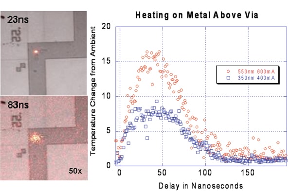
In order to test sub-nanosecond thermal imaging capability at small scales, a sample of test vias was used. Small vias can heat rapidly, and one can observe the heat diffusing into the metal. To detect the small change in reflection in very short times, active devices are thermally cycled and characterized with pulsed illumination and a boxcar averaging circuit. Thermal images are obtained for single vias which are 350nm and 550nm in diameter. The 550nm via is heated by pulsing currents up to 600mA at 50ns. While this is a high current density (~2×10⁸ A/cm2), the low duty cycle reduces the total power dissipation. Figure 1 shows the thermal images of a 550nm single via at 23ns and 83ns delay. During turn-on the temperature field is very localized near the via, however after turn-off the heat begins to diffuse into the metal. By using a small region, 25 pixels, in the thermal image one can step through the image series and determine the average temperature on top of the metal where the via is buried. The graph in Figure 1 shows the temperature for two different via sizes for the first 200ns, with a 50ns excitation pulse. The peak temperature is actually higher than the average presented. The red curve from the 550nm via was acquired at only 10sec per frame averaging, so that the entire curve was acquired in less than an hour. The blue curve from the 350nm via was acquired with 30sec averaging per frame, about 3 hours total. The advantage of the extra averaging is seen in the tail of the curves, where the blue trace shows less noise. The temperature sensitivity can be estimated at about 1°C, for a 30sec average.
Simultaneous Thermal and Electro-Luminescence Imaging of Solar Cells
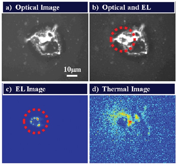
In order to identify and characterize various defects in thin-film amorphous-Si and copper indium gallium selenide (CIGS) solar cells, the device can be applied forward bias or applied reverse bias and thermal imaging can be performed. Typically lock-in infrared thermometry is used, which has micro Kelvin temperature resolution but the spatial resolution is limited to a few microns and one cannot detect visible light emission with the same long wavelength cameras. In the case of thermoreflectance it is possible to do simultaneous imaging of the visible electro-luminescence (EL) and the temperature distribution [11]. In this setup, we used a megapixel silicon-based CCD. EL can be indicative of pre-breakdown sites due to trap-assisted tunneling and stress-induced leakage currents. Many defects can be found through electroluminescence due to direct recombination. In solar cells, these EL defects are typically sites of avalanche breakdown and emit white light that can be detected by a silicon CCD. Figure 2 shows an avalanche defect with visible EL. Since the response time of the heat diffusion is very different from the electroluminescence response, we are able to separate the two effects using the same transient thermoreflectance imaging camera.
LED Imaging
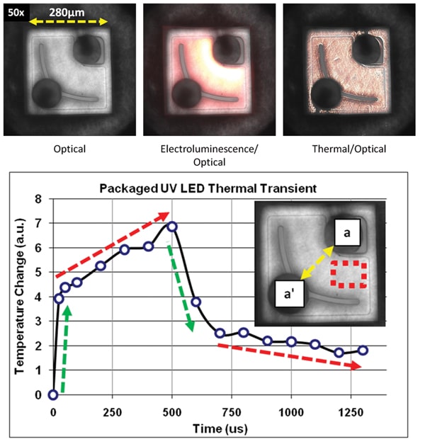
Non-uniformity of light emission within the active area of an LED device can be detected by an image sensor. Since LED devices are very sensitive to temperature thermal characterization of the active device provides useful information under both the steady-state and transient operations. Also, the details of temperature distribution are important to identify potential defects. Separation of the light emission from the device and the thermoreflectance signal is performed using a transient differencing algorithm and a precisely controlled phase delay [12]. Figure 3 shows the transient response to a step pulse drive current. The quick response of the metal surface is shown on the rising edge of the thermal transient (green arrow) within 25μs. The slower thermal transient of the package is shown by the red arrows.
CMOS Power Transistor Array
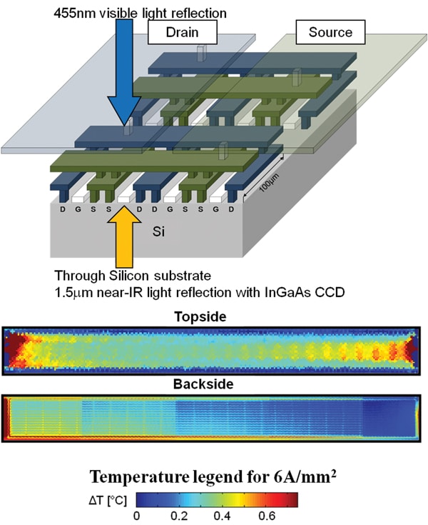
Performance and reliability in high current power transistors are strongly related to the peak temperature in the device. Device failure is linked to thermal rather than electrical effects. For power transistors with large areas or arrayed layouts, non-uniform current distribution throughout the device is common. Higher current density regions experience more self heating. If a local junction temperature exceeds critical levels anywhere in the power device, the structure as a whole may suffer parasitic electrical effects (e.g. gate leakage and snapback) or sustain irreversible damage (thermal runaway). A study on thermal profile in the depth of the device combined with software simulation has been reported by Raad [13]. Here we present rather direct thermal characterization of a large area of arrayed lateral diffused channels of the power MOSFETs with three layers of metallization [14]. The structure of the tested device is illustrated in Figure 4. The temperature of the top metal layer is measured with blue light illumination and the through-silicon thermal image is obtained using InGaAs camera with 1.5microns wavelength illumination. Thermal images from the topside and back side are very different. The topside image shows the temperature profile dominated by both the heat in the interconnect layer and the heat at the probes sending the current. The backside image shows the temperature profile in the transistor array. The non-uniformity and larger heating near the source contact can be detected.
Copper Interconnect Vias for Reliability
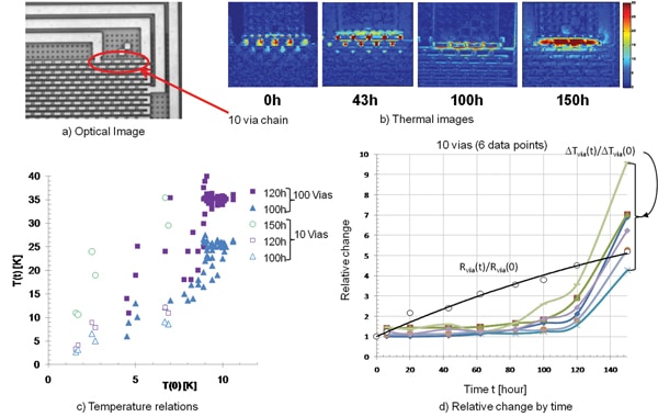
Thermal expansion mismatch among the different materials comprising integrated circuit chips results in significant tensile stress after high temperature cycles. Voiding and opening-circuit failure from the cracking of interconnects is one of the key failure mechanisms. This is particularly important in submicron copper interconnects. The thermal annealing is often used for accelerated aging for characterizing reliability (time-to-failure). Typically, total interconnect resistance is monitored as a function of aging at high temperatures. Increasing resistance is a sign of void formation but it cannot locate problematic areas. While techniques such as scanning electron microscopy can be used to locate open circuits, thermal imaging can detect the local change in each via’s resistance and in the thermal resistance of the surrounding material before a complete failure. Figures 5a-5d show the surface temperature rise of the 10 and 100 via chains under a bias before and after aging at 200°C for different durations [15]. Visible wavelength thermoreflectance gives 200-300nm spatial resolution. Localized heating in each of the 10 vias is 2-7°C before the thermal process. After 150 hours, this increases to 10-35°C (Figure 5b). During the aging the total resistance of the via chain increases linearly, a large change in the rate of the temperature increase is noticeable between 100 and 120 hours (Figure 5d). Close examination of the temperature profile shows significant change in the heat distribution pattern around the vias, which is a result of the void formation and the change in local thermal resistance. There is a strong correlation between local temperature rise in each via before high temperature treatment and that obtained after many hours of aging (Figure 5c). This would potentially shorten the time for reliability tests and suggest more specific solutions to improve reliability.
Summary
We explored our recent developments in ultrafast submicron thermoreflectance imaging techniques. This thermoreflectance was based on the change of a sample’s reflection coefficient as a function of temperature. Imaging with megapixel CCD cameras allowed precise detection of temperature distribution in a device. For ultrafast thermal measurements, resolution down to 800ps was achieved. With the use of near infrared illumination, it was possible to image through silicon substrates as thick as hundreds of microns. We also provided examples of thermal imaging in high power CMOS transistors, electrostatic discharge (ESD) devices, copper interconnects, LEDs, and solar cells.
References
[1] A. Cutolo, “Selected Contactless Optoelectronic Measurements for Electronic Applications,” Review of Scientific Instruments, Vol. 69, pp. 337-360, 1998.
[2] J. Altet, W. Claeys, S. Dilhaire, A. Rubio, “Dynamic Surface Temperature Measurements in ICs,”, to be published in the Proceedings of the IEEE, Vol. 94, No. 8, pp. 1519-1533, 2006.
[3] J. Christofferson, K. Maize, Y. Ezzahri, J. Shabani, X. Wang, and A. Shakouri, “Microscale and Nanoscale Thermal Characterization Techniques”, J. Electronic Packaging, Vol. 130, Issue 4, 041101, 2008.
[4] P. E. Raad, “Keeping Moore’s Law Alive”, Electronics Cooling, Vol. 16 No. 4, pp. 14-18, 2010.
[5] M. Farzaneh et al., “CCD-based thermoreflectance microscopy: principles and applications”, Journal of Physics D: Applied Physics 42, 143001 (20pp), 2009.
[6] M. G. Burzo, P. L. Komarov, P. E. Raad, “Thermo-Reflectance Thermography for Submicron Temperature Measurements”, Electronics Cooling, Vol. 14, February 1st, 2008.
[7] G. Tessier, S. Hole, and D. Fournier, “Quantitative Thermal Imaging By Synchronous Thermoreflectance With Optimized Illumination Wavelengths”, Applied Physics Letters, Vol. 78, No. 16: pp. 2267-2269, 2001.
[8] D. Lüerßen, J. A. Hudgings, P. M. Mayer, R. J. Ram, “Nanoscale thermo-reflectance microscopy with 10mK temperature resolution using stochastic resonance”, Proc. 21st Annual IEEE SEMI-THERM Symp. (San Jose, CA) pp 253-8, 2005.
[9] J. Christofferson and A. Shakouri, “Thermoreflectance Based Thermal Microscope”, Review of Scientific Instruments, 76, 024903-1-6, 2005.
[10] J. Christofferson, K. Yazawa, A. Shakouri, “Picosecond transient thermal imaging using a CCD based thermoreflectance system”, Proc. 14th International Heat Transfer Conference (IHTC14), 2010.
[11] D. Kendig, G.B. Alers, A. Shakouri, “Thermoreflectance imaging of defects in thin-film solar cells”, Proc. IEEE International Physics Reliability Symposium (IRPS), 2010.
[12] D. Kenig, A. Shakouri, “Thermal Imaging of Encapsulated LEDs”, 27th IEEE SEMI-THERM symposium, 2011
[13] P.E. Raad, P.L. Komarov, M.G. Burzo, “Numerical Simulation of Complex Submicron Devices”, Electronics Cooling, Vol. 15, pp. 18-22, May 2009.
[14] K. Maize, W. Xi, D. Kendig, A. Shakouri, W. French, B. O’Connell, P. Lindorfer, P. Hopper, “Thermal Characterization of High Power Transistor Arrays”, Proc. 25th IEEE SEMI-THERM Symposium, 2009.
[15] S. Alavi, K. Yazawa, G. Alers, B. Vermeersch, J. Christofferson, A. Shakouri, “Thermal Imaging for Reliability Characterization on High Precision Copper Vias in Silicon”, 27th IEEE SEMI-THERM symposium, 2011.


