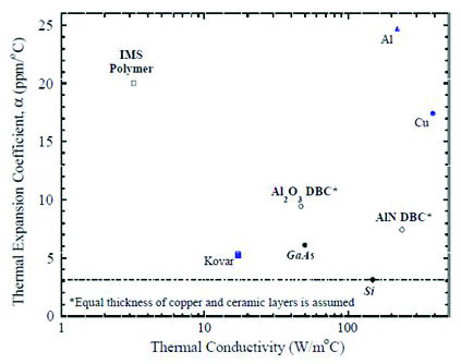
Expansion-matching materials development for semiconductor packaging has traditionally focused on ceramic, organic, metallic and composite materials used for packaging of silicon die for a broad variety of applications in many types of equipment markets. Market segments where these types of materials are used include integrated circuits, RF devices and components for communications, RF power amplifiers for phased-array radar and for military and aerospace communications and guidance components, power LEDs, optoelectronic modules, laser diodes and power semiconductors. A primary and continuing goal for materials development are material sets with similar coefficients of thermal expansion (CTE), within the specified operating temperature ranges required in these applications.
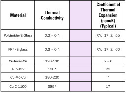
Mounting of active silicon power devices on substrates for these applications has led to the development of substrate materials referred to as direct bond copper (DBC) and direct bond aluminum (DBA) for ceramics, integrated metal substrates (IMS, insulated metal substrates) produced in organic printed circuit board manufacturing processes, and higher dielectric materials for higher frequency designs, and similar. These materials have been very successful for silicon device packaging and offer a range of thermal conductivity, CTE, dielectric properties, cost and other mechanical and electrical properties.

Newer semiconductor materials such as Gallium Nitride (GaN) and Silicon Carbide (SiC), with higher thermal conductivity and different CTE than Si and GaAs, require development of packaging materials that offer appropriate thermal properties, while also demonstrating improvements for manufacturability. The selection of materials made for a given device in an application is driven by reliability requirements and such factors as joining processes and joining materials, solder interconnections, fatigue failure potential under power and thermal cycling, maximum expected junction temperatures in transient and steady-state operating conditions; packaging density; package mounting and cooling; and cost. Reduction of CTE mismatch is critical to overall package reliability for many critical applications, especially with large and/or cyclical temperature gradients or significant overload conditions.
Development objectives
Development of GaAs and Gallium Nitride (GaN) semiconductor devices for RF and radar applications and Silicon Carbide (SiC) devices for high-temperature power devices is driving development of new substrate materials that have lower CTE values, similar to values for those semiconductor materials, and higher thermal conductivity (especially in the Z-axis). An important goal for cost and manufacturability is that new materials fit within existing PCB manufacturing processes. Reduced material weight is always important in aerospace and defense applications. A number of materials have been examined in one development program as candidates for development and production of organic PCBs with a high thermal conductivity, CTE-matched core.[1] Goals include manufacturability, process compatibility, and tested thermal performance capabilities of PCBs developed with new thermally-conductive core materials. One core material, a cast copper and graphite composite that has not previously been producible in large sheets (similar to what is required for PCB fabrication processes) was included in the development program. The manufacturer of the copper/graphite composite [2] subsequently developed manufacturing processes to allow production of 305mm x 457mm (12.0” x 18.0”) sheets of a thin version of this material. Following further process development, sheet thicknesses were reduced from the initial 1.02mm (0.040”) to the required 0.51mm (0.020”) to enable capture in-situ as a thermal core within organic multilayer PCBs for radar transceiver modules.

Results
Comparative testing of more traditional PCBs and newly-developed thermal core PCB materials in this program was conducted and results for production transceiver RF boards were evaluated. A detailed model of the test boards was prepared, to predict board thermal performance. Correlations were developed between modeling results and performance test data, with good results and close correlation values.
During the development phase for this program, one supplier continued to pursue a process investigation to determine if thinner sheet forms of the copper/graphite composite could be produced successfully and repeatably. This process development was successful and the required thickness was produced. Traditional PCB manufacturing processes require 457mm x 610mm (18”x24”) sheet forms of materials and the current stage of manufacturing process development for the copper/graphite composite has advanced to production of 457mm x 305mm (18” x 12”) sheet forms, which the participating PCB manufacturing firm, which has been leading the PCB development portion, has been able to accommodate.
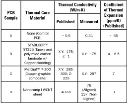
Additional materials examined and incorporated in the same PCB manufacturing process included a graphite composite thermal control material [4] in commercial PCBs, a long-walled carbon nanotube (LWCNT) sheet material [5], and others. Development PCB materials with these thermal control cores were manufactured successfully, as well as a control lot with no thermal control core.
In addition to thermal modeling of the core materials selected, a series of thermal imaging tests were conducted to develop a relative thermal merit map for thermal conductivity.
Additional printed circuit boards utilizing two of these materials will be manufactured for use in demonstration radar modules. The copper/graphite composite, with a measured thermal conductivity value that approaches that of copper alloys, also provides a matched CTE value that will allow, through the use of windows in the organic PCB material, direct mounting of RF devices on the thermal control layer. Note that MetGraf 7-300 has a Z-axis conductivity of 225 W/mK, a large improvement over other fabricated materials used as thermal cores, and has a high specific stiffness. Board construction consist of two layers of thermal control and 18-22 layers of organic and dielectric materials; this complexity makes direct measurement of CTE value for each test board construction difficult.
The selected materials, MetGraf 7-300 composite and the LWCNT, are also the subject of further development work between the two materials manufacturers to determine if future thermal management materials may be developed and manufactured.

Conclusions
Development of new PCB materials containing multiple thermal control layers has demonstrated higher thermal conductivity, high specific stiffness, and an approach to improvements in CTE matching for GaN and other semiconductor materials, and drop-in-place capability to match existing PCB manufacturing processes. All boards manufactured to date meet a PCB manufacturing industry standard, the IPC 6012 specification. Additional testing on the thinnest materials and to determine comparative improvements in junction temperatures with these materials will determine range of applicability for PCB applications with higher thermal performance requirements, CTE matching, lower weight, high specific stiffness, and applicability to existing manufacturing processes.
References
[1] Pergande, A., Rock, J., “Advances in Passive PCB Thermal Control,” Proceedings of the 2011 IEEE Aerospace Conference, Big Sky, Mont., March, 2011, manuscript 978-1-4244-7351-9/11.
[2] MetGraf™ 7-300, a trademark of MMCC Inc., Waltham, Mass.,
(www.mmccinc.com).
[3] J. He, V. Mehrotra, M. Shaw, Rockwell Science Center, Thousand Oaks, Calif. “Thermal Design and Measurements of IGBT Power Modules: Transient and Steady State.” Proceedings of IEEE IAS Conference, Phoenix Ariz., October 1999, pp. 1440-1444.
[4] STABLCOR® ST325 is a registered mark of Stablcor Technology Inc., Huntington Beach, Calif. (www.stablcor.com).
[5] Nanocomp Technologies Inc., Concord, N.H. (www.nanocomptech.com)
[6] IPC6012(C) “Qualification and Performance Specification for Rigid Printed Circuit Boards” (ISBN 1-580986-36-6), Released April 2010. Available from and published by IPC, Bannockburn IL, www.ipc.org


