Thermoelectric effects were discovered around 1830 by French and German scientists. Thomas Seebeck observed that a magnetic field was produced by a closed loop of two different metals with each junction having a different temperature. Soon after, Danish scientist Hans-Christian Oersted found the magnetic field to be caused by an electric current, so he assigned to Seebeck’s effect the term “thermoelectricity,” paving the way for solid state power generation.1 Some years later, in 1834, Jean Peltier discovered that between the junction points of the said loop of different metals a temperature difference is established when an electric power source forces current through the loop. Seebeck’s discovery made its way to the market mostly in the form of thermocouples and thermopiles used as temperature sensors and security switches for gas cookers. More significant power generation applications have left the planet, traveling to outer space where they provide power to deep space satellites, such as Explorer. During the past 50 years, commercial use has been made mostly from Peltier’s thermoelectric cooling effect in applications ranging from small refrigerator devices for camping and outdoor activities, cooled car seats and tin can holders to thermal management of tiny laser diodes used in fiberoptic telecom and datacom backhaul networks.
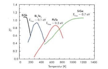
While all metals exhibit thermoelectric effects to some degree, semiconductors generally perform much better because they can be doped with additional charge carriers. Bismuth Telluride (Bi2Te3) is a semiconductor compound material that is grown in two flavors of large mono-crystals, one p-doped the other n-doped. P- and n-doped Bismuth Telluride elements have proven to be most efficient across the temperature range common in the human environment, up to 150°C approximately. The thermoelectric efficiency is a material property and referred to as the “Figure of Merit” ZT; it is basically derived from the voltage generated per temperature gradient and the ratio between thermal and electrical conductivity[1] as ZT = (S2 · σ/κ)·T, where σ is the electrical conductivity, S is Seebeck Coefficient (given in µV/K) and κ is thermal conductivity. T is the arithmetic average of the hot and cold temperatures at the ends of the thermocouple, (Th+Tc)/2.
The maximum value of ZT is found around 1 for most thermoelectrically active materials actually used, due to physical effects at the level of the crystalline lattice of those materials. Since the electrical conductivity of a good thermoelectric material should range somewhere between a metal and an insulator, it is not much of a surprise that almost all high performance thermoelectric bulk materials are semiconductors. ZT shows a material characterizing temperature dependency with a peak in a fairly narrow temperature range, found at levels between 100 and more than 1000 K (Figure 1). In order to obtain a higher ZT value for more efficient power generation, a high Seebeck coefficient S is required. This calls for a low thermal conductivity of the thermoelectric materials. Accordingly, the math for coolers demands that effective thermoelectric materials need to have a high Seebeck coefficient S, i.e. a high electrical conductivity and a small thermal conductivity at the same time. This, however, conflicts with the Wiedemann-Franz law [2] linking a higher electrical conductivity proportionally to a higher thermal conductivity.
As established production methods for thermoelectric semiconductor materials do not offer any means to affect the material properties which influence electrons and phonons as carriers of charge and heat, emerging thin film deposition technologies have been considered potential candidates for breaking into those structural dimensions. In the early 1990s fundamental research had identified low-dimensional structures[3] and their “configurable” thermal and electrical conduction properties as the long-sought handle on ZT – also see [4] for an overview of approaches.
Nanostructured Thermoelectric Materials
To overcome the ZT = 1 limit of homogeneous bulk materials, multiple nanostructured thin film materials have been investigated, because these materials offer design access at the dimensional level of both charge and heat carrier transport. An optimization of the thermoelectric figure of merit was considered possible using e.g. InPbTe or SiGe in a Multiple Quantum Well (MQW) structure, which was supposed to establish suitable barriers with ideally indefinite band gap and negligible electrical conductivity [5]. In bulk TE materials, ZT can only be optimized by varying the charge carrier concentration. MQW structures offer one more parameter for ZT optimization: the thickness of the quantum well. Theory predicted an increase of the figure of merit by more than a factor of 5. Soon these predictions were confirmed; compared to bulk materials (ZT of 0.2 at 400 K) two-dimensional quantum wells generated ZT values of up to 2 at 400 K. One problem remained, though. The entire thermoelectric structure necessarily had to include barrier layers whose poor thermoelectric properties fully contributed — negatively — to the overall ZT. As a result, the effective three-dimensional ZT values were found even smaller than those of homogeneous thin film materials. The initial model calculations also showed that one-dimensional structures, so called quantum wires, would allow for an even larger increase of ZT. However, such quantum wires would need to be embedded into matrix materials with a specific orientation to form mechanically stable thermoelectric layers. Like two-dimensional quantum wells, said matrix materials necessarily have poor thermoelectric properties. Consequently, materials with an effectively higher three-dimensional ZT have not yet been developed.
Current research trends include the combination of two good thermoelectric nanomaterials in layers, each with periodic structures. Interference effects of such layers promise to reduce thermal conductivity without inhibiting electrical conductivity. Another approach tries to leverage attractive thermoelectric properties of p-type Half-Heusler nano-sized cubes[6]. Reportedly, the good properties of individual Half-Heuslers initially give a 90% rise to ZT; however, this increase does not survive thermal treatment of the thermoelectric layers on their way to a functional device.
As of today, obviously, none of the activities which focus on substantial improvements of the thermoelectric Figure of Merit have resulted in a scalable industrial process and production technology which is indispensable to cater for large thermoelectric generators which would cover surfaces such as exhaust pipes, solar collectors and process equipment dissipating streams of waste heat — on a level that sensibly contributes to system efficiencies of those engines, thermal and solar power generation units, and many industrial processes. Hence, material choice is still limited to bulk materials and raw materials, and to what today’s process technology can do with them.
Thin Film Thermoelectric Devices
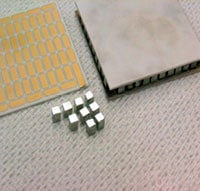
Ongoing miniaturization of electronics, largely condensed and increasingly three-dimensional circuitry calls for miniaturization of TE coolers, while the Seebeck law as such demands as many as possible thermocouples per area to generate high thermovoltages from small thermogenerators. Commercially available thermoelectric bulk devices for use around room temperature are produced by sawing wafer-like disks of thermoelectric materials into small cubes, referred to as “legs.” Arrays of alternating p- and n-legs are sandwiched and soldered between pre-metalized Al203 substrates (Figure 2). Neither dicing TE legs from brittle TE disks nor prevalent manual and semi-automated assembly processes lend themselves well towards miniaturization. The potentials of nanostructured thin film materials are open exclusively to thin film based processes which can provide the means for incorporating the distinct nano-structuring approaches discussed above and make them applicable to both small chip-sized devices for micro energy harvesting and large area heat recovery systems. Two general approaches for thin film TE device production have been established: in-plane legs and cross-plane legs. In-plane structures can produce high numbers of thermocouples, hence high voltages, but thermal resistance and consequently effective gradients across thin layers are low [7]. The electrical resistance of long aspect ratio TE structures, in addition, tends to be in the kilo Ohms, which in summary yields low microwatt power levels when integrated to chip scale [8]. This limitation may be overcome, though, by large area concepts.
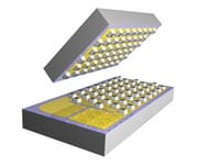
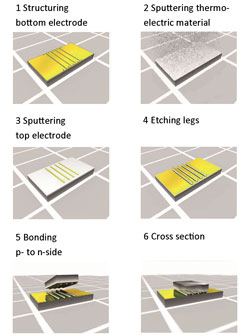
A cross-plane concept has been developed initially at the Freiburg, Germany-based Fraunhofer IPM. Established and matured process flows and production approaches obtain commercially viable thermoelectric thin film devices using a MEMS-like processing approach applying 4″ and 6″ wafers. While the same Bismuth Telluride-based compound semiconductor materials are being used, a proprietary thin film deposition process provides a viable platform to using nanostructured, high performance materials, once they become available. Wafers are processed by first depositing and patterning metal conductive structures (Figure 3.1), followed by an overgrowth with up to 36 microns of thermoelectric materials (Figure 3.2) covered by solder metals (Figure 3.3). Downstream the thermoelectric film is structured to form the entire array of p- or n- thermoelectric legs using photo masking and etching processes (Figure 3.4). Separate processes are required each for p- and n-type wafers. Flip chip bonding and bulk soldering of corresponding p-and n-type parts results in individual parts or arrays of functional device as shown in Figure 3.5. So-called tiles, consisting of arrays of devices, are separated into individual devices by another dicing process. In a bond process mating segments from p- and n-doped wafers are bonded to form one or multiple functional devices (Figure 4).
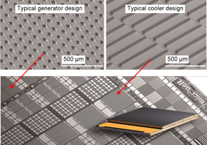
Structure geometries range from 30 µm to 600 µm feature sizes, as shown in Figure 5, providing a flexible platform for thermoelectric thin film devices matching the differing requirements requested by Seebeck generators and sensors or Peltier coolers respectively. Overall device geometries have been realized from footprints of 0.5 mm2 up to 25mm2.
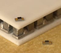
Figure 6 illustrates the size ratio of the smallest produced thin film TE cooler, featuring a cold side area well below 1 mm2, versus a legacy thermoelectric Peltier cooler: the thin film cooler easily fits on a single leg of the legacy bulk TEC. Across its effective leg height of as little as 36 µm the sputtered thermoelectric structure can establish an effective temperature difference of more than 60 K down from a hot side of 85°C. The same gradient across a 0.5 mm high TE leg would, theoretically, result in a ΔT of 850K. Theoretically, as 80% of the temperature difference of a legacy TEC is achieved along less than 5% of its respective height.
Micro-scale leg height and thermal mass of thin film coolers provide benefits to many applications. The thermal resistance of thin film TE devices is very low, leading to high cooling power densities of up to 100W/cm2 (650 W/sq in) — over 10 times more than conventional bulk TE devices. Such high heat flux densities — in concert with small associated thermal masses — allow for improved dynamics of thermal control, applicable to sub-square millimeters of footprint. Temperature levels of small amounts of material can be “switched” rather than being ramped up and down. With no thermal load attached, temperature change rates of up to 180°C per second are achieved. Thermal loads with 100 times the thermal capacity of the driving thin film cooler can be controlled at heating and cooling rates in the range of 10-20°C/s. This level of performance qualifies micro coolers as an ideal ‘engine’ for fast and accurate temperature control of sensors, thermal management of small devices and distinct hot spots, and for thermal cycling of genetic material samples down to chip level.
Following the imminent needs for further reduction of size, power consumption and cost of thermoelectric cooling systems a variation of a TEC was developed to optimally match the larger system scope of the TEC including its associated drive circuit. Small power TECs suffer from low electrical resistances below 1 Ohm. This leads to low power regulator efficiencies of the driver circuit which often has to supply well over 1 A of current to this low resistance load. Large amounts of additional waste heat are being produced in such high current cooling systems, characterized by low overall coefficients of performance (COP).
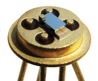
The inherent structural scaling flexibility of thermoelectric thin films supports optimized matching of the TEC’s electrical resistance to low current drive components, letting them operate at a high level of electrical efficiency. A photomask set is needed to produce the respective TEC micro structure with size and number of thermocouples that creates a resistance of about 30 Ohms. Required structural dimensions are determined by numerical simulation based on the well-known properties of the sputtered thin film material. The resulting TEC device (Figure 7) consumes only 200 mA for pumping 600 mW of heat. The drive voltage of around 3 Volt is readily available in most electronic systems which require some amount of thermal management on a square millimeter scale. The designed impedance match yields an electrical efficiency of the low cost small footprint drive circuit near 90%. The total power consumption for of the entire TEC/driver combo is about 50% of a comparable legacy design. Since the device’s maximum delta T is limited to little over 30 K, applications are likely found in VCSEL (Vertical Cavity Surface Emitting Laser: solid state lasers with beam emission perpendicular to its surface, typically low power) and small edge emitter laser systems which only require limited temperature offsets but both highly dynamic and precise control enabled by the low thermal mass of a silicon based micro TEC.
While thermoelectric nano-structured materials still require considerable development efforts to reach commercial viability, venture capital is presently funding the world’s first volume fab for thermoelectric thin film products in the German city of Halle/Saale. The upcoming additional device capacity of 5 to 10 million micro coolers and thermogenerators will likely not have much effect on the established markets of bulk thermoelectrics and their well-established and proven application fields. Assembly automation of bulk TE will continue to drive cost down and likely also the minimum size of TE legs. Choosing between bulk and thin film is getting more difficult at the overlap of both technologies. Expectations in thin film TE are focusing primarily on Seebeck devices which provide micro- and milliwatts of power to autonomous wireless sensors and other micro systems incorporated in very compact thermal paths of high power density. Strong growth expectations in this market are driven by largely increased pressure on reduction of energy consumption, status information based asset management and expanding building automation. Micro TECs will benefit from this volume driver through lower cost and quality levels common to chip production. Less defensive applications of micro TECs in particular are expected to emerge big time in life sciences where disposable narrow band genetic testing is seen at every doctor’s desk helping to identify specific diseases faster and help matching medication to a patient on an individual basis. Why less defensive? A laser system can always be specified or improved to work without a cooler — saving megawatts across all installed devices. A one-off genetic test worth the energy of a light bulb running for an hour, however, can save a life — and in many cases it can’t run at the desirable dynamic level without a micro TEC for thermal cycling.
References
[1] Sootsman, J., Chung, D., Kanatzidis M., Angew. Chem. Int. Ed. 2009, 48, 8616-8639.
[2] Lasance, C., “How Thermal Conductivity Relates to Electrical Conductivity,” ElectronicsCooling, May 2000.
[3] Hicks, L.D., Dresselhaus, M.S., “Effect of Quantum-weH Structures on the Thermoelectric Figure of Merit,” Phys. Rev. B 47(19). 12727-12731 (1993).
[4] Lasance, C., Simons, R.E., “Advances in High-Performance Cooling for Electronics, ElectronicsCooling, November 2005.
[5] Numus, J., Böttner, H., Lambrecht, A., Chapter 48 in: Thermoelectrics Handbook: Macro to Nano: Nanoscale Thermoelectrics, ISBN 0-8493-2264-2.
[6] Xiao Yan, Giri Joshi, Weishu Liu, Yucheng Lan, Hui Wang, Sangyeop Lee, J. W. Simonson, S. J. Poon, T. M. Tritt, Gang Chen, and Z. F. Ren in Nano Lett, 2011, 11 (2), pp 556–560.
[7] Leonov, V., Van Hoof, C., Vullers, R., “Thermoelectric and Hybrid Generators in Wearable Devices and Clothes,” bsn, pp. 195-200, 2009; Sixth International Workshop on Wearable and Implantable Body Sensor Networks, 2009.
[8] Leonov, V., Van Hoof, C., Vullers, R., “Thermoelectric and Hybrid Generators in Wearable Devices and Clothes,” Proceedings of the 2009 Sixth International Workshop on Wearable and Implantable Body Sensor Networks.


