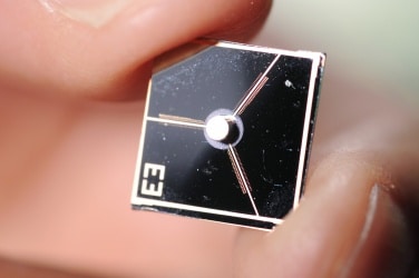
 Researchers at the Georgia Institute of Technology have developed a new technique for measuring the adhesion strength between thin films of materials used in microelectronic devices, photovoltaic cells and MEMS using magnetic repulsion.
The fixtureless and noncontact technique, known as the magnetically actuated peel test (MAPT), could help ensure the long-term reliability of electronic devices, and assist designers in improving resistance to thermal and mechanical stresses.
Modern microelectronic chips are fabricated from layers of different materials – insulators and conductors – applied on top of one another. Thermal stress can be created when heat generated during the operation of the devices causes the materials of adjacent layers to expand, which occurs at different rates in different materials. The stress can cause the layers to separate, a process known as delamination or de-bonding, which is a major cause of microelectronics failure.
Sitaraman and doctoral student Gregory Ostrowicki have used their technique to measure the adhesion strength between layers of copper conductor and silicon dioxide insulator. They also plan to use it to study fatigue cycling failure, which occurs over time as the interface between layers is repeatedly placed under stress. The technique may also be used to study adhesion between layers in photovoltaic systems and in MEMS devices.


