Thermal design and material selection continues to be a concern for electronic packages, particularly for flip chip ball grid array packages (FCBGA). Lower cost package options are available today, which are finding applications in high power design spaces that previously only employed copper lid heat spreaders. Exposed die flip chip packages are used frequently in lower power applications where the die size is relatively small (less than 8mm). Larger die sizes exhibit greater package warpage due to the difference in thermal expansion coefficients between silicon and laminate materials. As a result, large die packages are more difficult to solder mount and may produce larger variations in the bond line thickness between the die and external heat sinks. Two options are available to reduce the package warpage. The first option, shown in Figure 1(a), is to mount a stiffener window to the periphery of the package in order to provide structural rigidity. A second and lower cost option is to underfill the die and mold the body of the package in a single process step. This style of package, as shown in Figure 1(b), is called a flip chip molded ball grid array (FCmBGA). The most common style of package is the flip chip lidded ball grid array (FCLBGA), as shown in Figure 1(c). A copper lid is mounted to the die back-side with thermal interface material (TIM I) between the lid and die. An added benefit of the exposed die package options, Figure 1(a) and 1(b), is the elimination of the thermal interface material (TIM I). For exposed die packages, only one interface is needed (TIM II) between the die and heat sink.
Table 1. Heat sink description.

Experimental Measurements
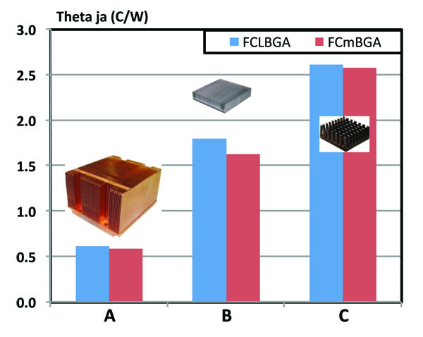
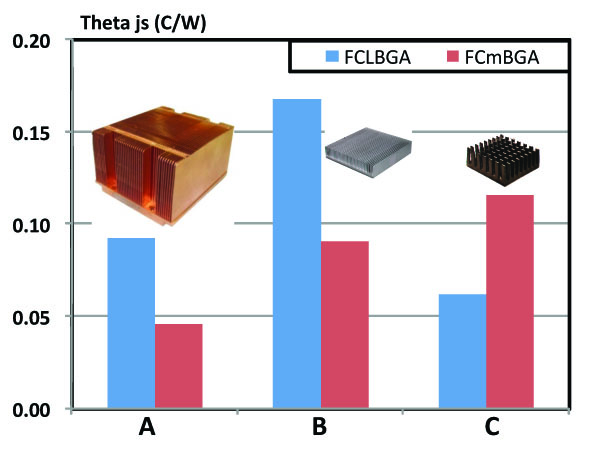
This study reports measurements made with FCmBGA and FCLBGA packages as a function of heat sink size. Both styles of packages have a 45mm body size with an 18mm die. Experimental measurements were made using packages shown in Figure 1(b) and 1(c) with three different size heat sinks as described in Table 1. A relatively low thermal resistance TIM II, 15C- mm2/W, was used to gather the data reported here. A more detailed description may be found in Galloway and Kanuparthi [1]. Theta js is defined as the maximum junction temperature (measured at center of die), less the heat sink temperature (measured at a location centered on the heat sink base), divided by the supplied power. Theta js is useful in characterizing the performance of the package and TIM II. The FCmBGA style package has a lower thermal resistance when the heat sink base can adequately spread the heat, see Figure 2(a). A thicker heat sink base with a higher conductivity material promotes greater spreading of heat away from the die. Heat sink C has a relatively thin base and is made from a lower conductivity material (aluminum). As a result the lidded package, even though it has an additional TIM layer, produces a lower Theta js due to the design of heat sink C. Theta ja provides a measurement of the total resistance including the combined resistance of the heat sink, TIM II and package, see Figure 2(b). A slight reduction in Theta ja was measured for heat sinks A and B with the FCmBGA package. Theta js is approximately 25X lower than Theta ja for heat sink C. Hence no appreciable differences in Theta ja was measured for heat sink C even though Theta js was lower for the FCLBGA package.

Numerical Simulations
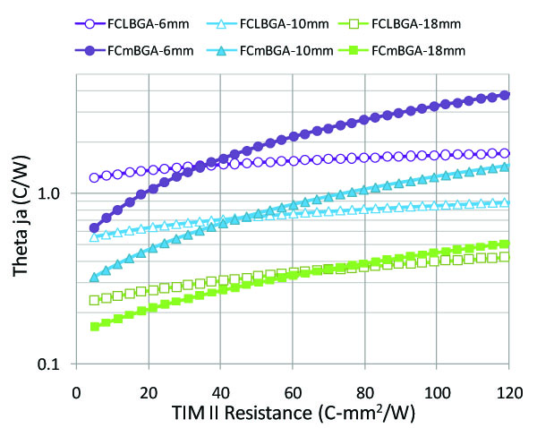
To provide a more detailed understanding of the impact of TIM II material on Theta ja, a finite element analysis (FEA) study was conducted to predict Theta ja as a function of package style (FCLBGA versus FCmBGA) and TIM II resistance for 6mm,
10mm and 18mm die. As one may expect, for low TIM II resistance, the FCmBGA package provides the lowest thermal resistance since there is only one interface (TIM II) whereas the FCLBGA has two interfaces, TIM I and TIM II.

The TIM II interface can become a dominant factor if the bond line thickness (BLT) is large. In certain cases, system level designs cannot control the BLT at the TIM II layer due to component stack-up variations, e.g. when the de facto heat sink is an EMI shield or a system chassis. For these cases, a gap filler TIM II must be used. Gap filler TIMs, as their name suggests, are relatively thick/low modulus materials that conform to the gap available between the package top surface and the heat sink. FCmBGA Theta ja variation with TIM II resistance has a steeper slope compared to the FCLBGA package. Adding a lid tends to spread the heat over an area larger than the die, thus reducing the TIM II resistance. However, for larger die sizes, the difference between FCLBGA and FCmBGA Theta ja becomes smaller. The Theta ja resistance cross-over point, where the FCLBGA resistance is equal to the FCmBGA package, occurs at a TIM II resistance of approximately 45oC- mm2/W.
Conclusion
The FCmBGA package style offers an attractive means for reducing the overall package resistance. To achieve these benefits, a lower resistance TIM II material will be required.
References
[1] Galloway J. and S. Kanuparthi, “Thermal performance of FCmBGA: Exposed molded die compared to lidded package” Semiconductor Thermal Measurement and Management Symposium (SEMI-THERM), 2011, 27th Annual IEEE, March 2011, pp. 181 – 186.


